NLMD5820MUTAG ON Semiconductor, NLMD5820MUTAG Datasheet
NLMD5820MUTAG
Specifications of NLMD5820MUTAG
Available stocks


Related parts for NLMD5820MUTAG

NLMD5820MUTAG Summary of contents
Page 1
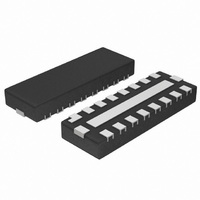
... PDAs and Smart Phones © Semiconductor Components Industries, LLC, 2007 September, 2007 - Rev. 0 resistance 2 5 NLMD5820MUTAG For information on tape and reel specifications, including part orientation and tape sizes, please refer to our Tape and Reel Packaging Specification Brochure, BRD8011/D. 1 http://onsemi.com MARKING ...
Page 2
INM i BYPASS Required Negative for Differential BYPASS Filtering Input the Audio INTERNAL Input BIASING Signal BYPASS INP R NC1 Positive COM1 Differential NC2 Input COM2 NLMD5820 2 ...
Page 3
PIN DESCRIPTION Pin No. Symbol Type 1 NC2 I/O Normally Closed Signal Line for Switch #2. 2 IN2 I Control Input for Switch #2. 3 COM2 I/O Common Signal Line for Switch # Analog Supply for Switches. ...
Page 4
MAXIMUM RATINGS Symbol V Supply Voltage for Amplifier p V Input Voltage for Amplifier in V Supply Voltage for Switches CC V Analog Signal Voltage for Switches ( Control Input for Switches IN I Max Output Current of ...
Page 5
ELECTRICAL CHARACTERISTICS OF AMPLIFIER Characteristic Supply Quiescent Current Shutdown Current Shutdown Voltage High Shutdown Voltage Low Switching Frequency Gain Output Impedance in Shutdown Mode Resistance from SD to GND Output Offset Voltage Turn On Time Turn Off Time Thermal Shutdown ...
Page 6
ELECTRICAL CHARACTERISTICS OF AMPLIFIER Characteristic Total Harmonic Distortion + Noise Common Mode Rejection Ratio Power Supply Rejection Ratio DC ELECTRICAL CHARACTERISTICS OF SWITCHES Characteristic Control Input High Voltage Control Input Low Voltage Control Input Leakage Current ON State Leakage Current ...
Page 7
AC ELECTRICAL CHARACTERISTICS OF SWITCHES Symbol Parameter t Turn-On Time ON t Turn-Off Time OFF C Control Pin Input Capacitance Port Capacitance NC C COM Port Capacitance When Switch is COM Enabled BW Maximum On-Channel -3 dB ...
Page 8
TYPICAL CHARACTERISTICS OF AMPLIFIER 100 90 80 NLMD5820 Class 0.2 0.4 0.6 P (W) out Figure 3. Efficiency vs kHz ...
Page 9
TYPICAL CHARACTERISTICS OF AMPLIFIER 90 80 NLMD5820 Class 0.2 0.4 0.6 P (W) out Figure 9. Efficiency vs kHz V = 3.6 V, ...
Page 10
TYPICAL CHARACTERISTICS OF AMPLIFIER 2 kHz 1.0 NLMD5820 0.1 0.01 0 0.1 0.2 P (W) out Figure 15. THD+N vs. Pout = ...
Page 11
TYPICAL CHARACTERISTICS OF AMPLIFIER 2 kHz 1.5 NLMD5820 THD+N = 10% 1.0 0.5 0 2.5 3.0 3.5 4.0 POWER SUPPLY (V) Figure 21. Output Power vs. Power Supply = ...
Page 12
TYPICAL CHARACTERISTICS OF AMPLIFIER -20 -30 -40 -50 -60 -70 -80 10 100 1000 FREQUENCY (Hz) Figure 27. PSRR vs. Frequency = 8 W, Vic = 200 mvpkpk 900 = 8 W 800 ...
Page 13
TYPICAL CHARACTERISTICS OF AMPLIFIER +85° +25° -40° 2.5 3.5 POWER SUPPLY (V) Figure 33. Turn on Time TYPICAL CHARACTERISTICS OF SWITCHES 0 -10 -20 -30 ...
Page 14
TYPICAL CHARACTERISTICS OF SWITCHES 0.12 0.1 0.08 0.06 0.04 0. 100 1000 FREQUENCY (Hz) Figure 37. Total Harmonic Distortion 0.4 0.35 0.3 85°C 0.25 25°C 0.2 -40°C 0.15 0.1 0. 0.5 1 1.5 2 2.5 V ...
Page 15
DUT V Output CC 0 Switch Select Pin DUT V Output CC 0.1 mF Open Input DUT Output Open Input NLMD5820 V CC Input GND V OUT 35 pF Output GND Figure 42. t (Time Break-Before-Make) BBM ...
Page 16
W Generator Channel switch control/s test socket is normalized. Off isolation is measured across an off channel. On loss is the bandwidth switch. V ISO V = Off Channel Isolation = 20 Log ISO V = ...
Page 17
Detailed Description The basic structure of the amplifier portion of the NLMD5820 is composed of one analog pre-amplifier, a pulse width modulator and an H-bridge CMOS power stage. The first stage is externally configurable with gain-setting resistor R and the ...
Page 18
NLMD5820 PWM Modulation Scheme The NLMD5820 uses a PWM modulation scheme with each output switching from 0 to the supply voltage outputs OUTM and OUTP are in phase and no current is flowing through the differential ...
Page 19
OUTM 2.2 mF 2.2 mF OUTP 15 mH Figure 48. Advanced Optional Audio Output Filter Figure 50. Optional EMI Ferrite Bead Filter Differential Audio Input from DAC Input from Microcontroller Figure 51. NLMD5820 Application Schematic with Fully Differential ...
Page 20
C i Differential Audio Input from DAC C i Input from Microcontroller Figure 53. NLMD5820 Application Schematic with Differential Input Configuration and Single-Ended Audio Input from DAC Microcontroller Figure 54. NLMD5820 Application Schematic with Single Ended Input Configuration C i ...
Page 21
... A B *For additional information on our Pb-Free strategy and soldering 0.05 C NOTE 3 details, please download the ON Semiconductor Soldering and Mounting Techniques Reference Manual, SOLDERRM/D. N. American Technical Support: 800-282-9855 Toll Free USA/Canada Europe, Middle East and Africa Technical Support: Phone: 421 33 790 2910 Japan Customer Focus Center ...