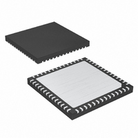
MAX9709ETN+TD Maxim Integrated Products, MAX9709ETN+TD Datasheet - Page 15

MAX9709ETN+TD
Manufacturer Part Number
MAX9709ETN+TD
Description
IC AMP AUDIO PWR 50W STER 56TQFN
Manufacturer
Maxim Integrated Products
Type
Class Dr
Datasheet
1.MAX9709ETND.pdf
(20 pages)
Specifications of MAX9709ETN+TD
Output Type
1-Channel (Mono) or 2-Channel (Stereo)
Max Output Power X Channels @ Load
50W x 1 @ 4 Ohm; 29W x 2 @ 8 Ohm
Voltage - Supply
10 V ~ 22 V
Features
Depop, Differential Inputs, Mute, Short-Circuit and Thermal Protection, Shutdown
Mounting Type
Surface Mount
Package / Case
56-TQFN
Lead Free Status / RoHS Status
Lead free / RoHS Compliant
In certain systems, a single audio source can be
shared by multiple devices (speaker and headphone
amplifiers). When sharing inputs, it is common to mute
the unused device, rather than completely shutting it
down. This prevents the unused device inputs from dis-
torting the input signal. Mute the MAX9709 by driving
MUTE low. Driving MUTE low turns off the Class D out-
put stage, but does not affect the input bias levels of
the MAX9709.
The MAX9709 outputs up to 27W on each channel in
stereo mode. If higher output power or a 2.1 solution is
needed, two MAX9709s can be used. Each MAX9709
is synchronized by connecting SYNCOUT from the first
MAX9709 to SYNCIN of the second MAX9709 (see
Figure 5).
Proper power-supply bypassing ensures low distortion
operation. For optimum performance, bypass PV
PGND with a 0.1µF capacitor as close to each PV
pin as possible. A low-impedance, high-current power-
supply connection to PV
capacitance should be added, as required, depending
on the application and power-supply characteristics.
GND and PGND should be star-connected to system
ground. For the TQFN package, solder the exposed
paddle (EP) to the ground plane using multiple-plated
through-hole vias. The exposed paddle must be sol-
dered to the ground plane for rated power dissipation
and good ground return. Use wider PC board traces to
lower the parasitic resistance for the high-power output
pins (OUTR+, OUTR-, OUTL+, OUTL-). Refer to the
MAX9709 evaluation kit for layout guidance.
Class D amplifiers provide much better efficiency and
thermal performance than a comparable Class AB
amplifier. However, the system’s thermal performance
must be considered with realistic expectations along
with its many parameters.
______________________________________________________________________________________
Frequency Synchronization
25W/50W, Filterless, Spread-Spectrum,
DD
Thermal Considerations
Sharing Input Sources
is assumed. Additional bulk
Supply Bypassing/Layout
Stereo/Mono, Class D Amplifier
DD
DD
to
When a Class D amplifier is evaluated in the lab, often
a continuous sine wave is used as the signal source.
While this is convenient for measurement purposes, it
represents a worst-case scenario for thermal loading
on the amplifier. It is not uncommon for a Class D
amplifier to enter thermal shutdown if driven near maxi-
mum output power with a continuous sine wave. The
PC board must be optimized for best dissipation (see
the PC Board Thermal Considerations section).
Audio content, both music and voice, has a much lower
RMS value relative to its peak output power. Therefore,
while an audio signal may reach similar peaks as a
continuous sine wave, the actual thermal impact on the
Class D amplifier is highly reduced. If the thermal per-
formance of a system is being evaluated, it is important
to use actual audio signals instead of sine waves for
testing. If sine waves must be used, the thermal perfor-
mance is less than the system’s actual capability for
real music or voice.
The exposed pad is the primary route for conducting
heat away from the IC. With a bottom-side exposed
pad, the PC board and its copper becomes the primary
heatsink for the Class D amplifier. Solder the exposed
pad to a copper polygon. Add as much copper as pos-
sible from this polygon to any adjacent pin on the Class
D amplifier as well as to any adjacent components, pro-
vided these connections are at the same potential.
These copper paths must be as wide as possible. Each
of these paths contributes to the overall thermal capa-
bilities of the system.
The copper polygon to which the exposed pad is
attached should have multiple vias to the opposite side
of the PC board, where they connect to another copper
polygon. Make this polygon as large as possible within
the system’s constraints for signal routing.
Additional improvements are possible if all the traces
from the device are made as wide as possible.
Although the IC pins are not the primary thermal path
out of the package, they do provide a small amount.
The total improvement would not exceed about 10%,
but it could make the difference between acceptable
performance and thermal problems.
PC Board Thermal Considerations
Continuous Sine Wave vs. Music
15


