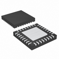
MAX9714ETJ+ Maxim Integrated Products, MAX9714ETJ+ Datasheet - Page 11

MAX9714ETJ+
Manufacturer Part Number
MAX9714ETJ+
Description
IC AMP AUDIO PWR 8W STER 32TQFN
Manufacturer
Maxim Integrated Products
Type
Class Dr
Datasheet
1.MAX9713ETJ.pdf
(18 pages)
Specifications of MAX9714ETJ+
Output Type
2-Channel (Stereo)
Max Output Power X Channels @ Load
8W x 2 @ 16 Ohm
Voltage - Supply
10 V ~ 25 V
Features
Depop, Differential Inputs, Mute, Short-Circuit and Thermal Protection, Shutdown
Mounting Type
Surface Mount
Package / Case
32-TQFN Exposed Pad
Product
Class-D
Output Power
6 W
Common Mode Rejection Ratio (min)
60 dB
Thd Plus Noise
0.07 %
Supply Current
18 mA
Maximum Power Dissipation
2963 mW
Maximum Operating Temperature
+ 85 C
Mounting Style
SMD/SMT
Audio Load Resistance
8 Ohms
Minimum Operating Temperature
- 40 C
Lead Free Status / RoHS Status
Lead free / RoHS Compliant
The value of the flying capacitor (C1) affects the load
regulation and output resistance of the charge pump. A
C1 value that is too small degrades the device’s ability to
provide sufficient current drive. Increasing the value of
C1 improves load regulation and reduces the charge-
pump output resistance to an extent. Above 1µF, the on-
resistance of the switches and the ESR of C1 and C2
dominate.
The output capacitor value and ESR directly affect the
ripple at CHOLD. Increasing C2 reduces output ripple.
Likewise, decreasing the ESR of C2 reduces both rip-
ple and output resistance. Lower capacitance values
can be used in systems with low maximum output
power levels.
The MAX9713/MAX9714 do not require an output filter.
The device passes FCC emissions standards with
36cm of unshielded speaker cables. However, output
filtering can be used if a design is failing radiated emis-
sions due to board layout or cable length, or the circuit
is near EMI-sensitive devices. Use a ferrite bead filter
when radiated frequencies above 10MHz are of con-
cern. Use an LC filter when radiated frequencies below
10MHz are of concern, or when long leads connect the
TOP VIEW
OUT+
OUT+
OUT-
OUT-
N.C.
N.C.
N.C.
N.C.
______________________________________________________________________________________
25
26
27
28
29
30
31
32
+
24
1
23 22
TQFN (5mm x 5mm)
2
3
MAX9713
Output Capacitor (C2)
21
Flying Capacitor (C1)
4
20 19 18 17
5
6W, Filterless, Spread-Spectrum
6
Mono/Stereo Class D Amplifiers
Output Filter
7
8
16 G2
15
14
13
12
11
10
9
G1
SHDN
SS
IN+
IN-
AGND
REG.
amplifier to the speaker. Refer to the MAX9714
Evaluation Kit schematic for details of this filter.
In certain systems, a single audio source can be shared
by multiple devices (speaker and headphone ampli-
fiers). When sharing inputs, it is common to mute the
unused device, rather than completely shutting it down,
preventing the unused device inputs from distorting the
input signal. Mute the MAX9713/MAX9714 by driving SS
low through an open-drain output or MOSFET (see the
System Diagram). Driving SS low turns off the Class D
output stage, but does not affect the input bias levels of
the MAX9713/MAX9714. Be aware that during normal
operation, the voltage at SS can be up to 7V, depending
on the MAX9713/MAX9714 supply.
Proper power-supply bypassing ensures low distortion
operation. For optimum performance, bypass V
PGND with a 0.1µF capacitor as close to each V
as possible. A low-impedance, high-current power-sup-
ply connection to V
capacitance should be added as required depending on
the application and power-supply characteristics. AGND
and PGND should be star connected to system ground.
Refer to the MAX9714 Evaluation Kit for layout guidance.
MAX9713 TRANSISTOR COUNT: 3093
MAX9714 TRANSISTOR COUNT: 4630
PROCESS: BiCMOS
OUTR+
OUTR+
OUTL+
OUTL+
OUTR-
OUTR-
OUTL-
OUTL-
25
26
27
28
29
30
31
32
+
24
1
23 22
2
TQFN (7mm x 7mm)
3
MAX9714
21
4
DD
20 19 18 17
5
is assumed. Additional bulk
Pin Configurations
6
Sharing Input Sources
Supply Bypassing/Layout
Chip Information
7
8
16 INR+
15
14
13
12
11
10
9
INR-
REG.
AGND
SS
SHDN
INL+
INL-
DD
DD
pin
11
to


