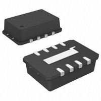
AD8317ACPZ-R7 Analog Devices Inc, AD8317ACPZ-R7 Datasheet - Page 12

AD8317ACPZ-R7
Manufacturer Part Number
AD8317ACPZ-R7
Description
IC AMP LOG DETECT 8GHZ 8-LFCSP
Manufacturer
Analog Devices Inc
Type
Logarithmic Amplifierr
Datasheet
1.AD8317ACPZ-R7.pdf
(20 pages)
Specifications of AD8317ACPZ-R7
Applications
Receiver Signal Strength Indication (RSSI)
Mounting Type
Surface Mount
Package / Case
8-LFCSP
No. Of Amplifiers
1
Dynamic Range, Decades
55
Response Time
20ns
Supply Voltage Range
3V To 5.5V
Amplifier Case Style
LFCSP
No. Of Pins
8
Supply Current
22mA
Lead Free Status / RoHS Status
Lead free / RoHS Compliant
Other names
AD8317ACPZ-R7TR
AD8317
The slope is given by
For example, if a resistor divider to ground is used to generate a
V
or −44 mV/dB.
TEMPERATURE COMPENSATION OF OUTPUT
VOLTAGE
The primary component of the variation in V
as the input signal amplitude is held constant, is the drift of the
intercept. This drift is also a weak function of the input signal
frequency; therefore, provision is made for the optimization of
internal temperature compensation at a given frequency by
providing Pin TADJ.
R
this resistor partially determines the magnitude of an analog
correction coefficient, which is used to reduce intercept drift.
The relationship between output temperature drift and
frequency is not linear and cannot be easily modeled. As a
result, experimentation is required to choose the correct
TADJ resistor. Table 4 shows the recommended values for
some commonly used frequencies.
Table 4. Recommended R
Frequency
50 MHz
100 MHz
900 MHz
1.8 GHz
1.9 GHz
2.2 GHz
3.6 GHz
5.3 GHZ
5.8 GHz
8 GHz
MEASUREMENT MODE
When the V
back to the VSET pin, the device operates in measurement
mode. As seen in Figure 27, the AD8317 has an offset voltage,
a negative slope, and a V
end of its input signal range.
TADJ
SET
−I
voltage of V
is connected between TADJ and ground. The value of
D
× 2x × 1.5 kΩ = −22 mV/dB × x
R
TADJ
OUT
voltage or a portion of the V
OUT
TADJ
/2, x = 2. The slope is set to −880 V/decade
Figure 26. TADJ Interface
V
OUT
INTERNAL
Recommended R
18 kΩ
18 kΩ
18 kΩ
8 kΩ
8 kΩ
8 kΩ
8 kΩ
500 Ω
500 Ω
Open
COMM
TADJ
measurement intercept at the high
Values
1.5k
COMM
Ω
AD8317
TADJ
I
COMP
OUT
OUT
vs. temperature,
voltage is fed
Rev. B | Page 12 of 20
The output voltage vs. input signal voltage of the AD8317 is
linear-in-dB over a multidecade range. The equation for this
function is
where:
X is the feedback factor in V
V
V
the V
V
An offset voltage, V
the detector signal, so that the minimum value for V
X × V
The slope is very stable vs. process and temperature variation.
When base-10 logarithms are used, V
volts/decade. A decade corresponds to 20 dB; V
V
As noted in Equation 3 and Equation 4, the V
negative slope. This is also the correct slope polarity to control
the gain of many power amplifiers in a negative feedback con-
figuration. Because both the slope and intercept vary slightly
with frequency, it is recommended to refer to the Specifications
section for application-specific values for slope and intercept.
Although demodulating log amps respond to input signal
voltage, not input signal power, it is customary to discuss the
amplitude of high frequency signals in terms of power. In this
case, the characteristic impedance of the system, Z
known to convert voltages to their corresponding power levels.
The following equations are used to perform this conversion:
SLOPE/DEC
INTERCEPT
INTERCEPT
SLOPE/dB
1.75
2.00
1.50
1.25
1.00
0.75
0.50
0.25
V
= X × V
P [dBm] = 10 × log
P [dBV] = 20 × log
P [dBm] = P [dBV] − 10 × log
–60 –55 –50 –45 –40 –35 –30 –25 –20 –15 –10 –5
0
OUT
OFFSET
OUT
represents the slope in volts/dB.
vs. P
is nominally −440 mV/decade, or −22 mV/dB.
is the x-axis intercept of the linear-in-dB portion of
is 2 dBV for a sinusoidal input signal.
= X × V
; therefore, for X = 1, the minimum V
Figure 27. Typical Output Voltage vs. Input Signal
SLOPE/dB
IN
curve (see Figure 27).
SLOPE/DEC
× 20 × log
OFFSET
SLOPE AND INTERCEPT
10
CALCULATION OF
10
, of 0.35 V is internally added to
(V
(V
× log
RANGE FOR
V
V
ERROR 25°C
RMS
P
OUT
RMS
SET
OUT
IN
10
/1 V
(dBm)
10
2
(V
IDEAL
= V
/(Z
25°C
(V
IN
0
IN
RMS
10
/V
OUT
× 1 mW))
(Z
/V
INTERCEPT
SLOPE/DECADE
)
/X.
0
INTERCEPT
× 1 mW/1 V
)
OUT
)
0
SLOPE/DECADE
represents the
OUT
voltage has a
0
5
, must be
is 0.35 V.
OUT
RMS
10
INTERCEPT
2.0
1.5
1.0
0.5
0
–0.5
–1.0
–1.5
2
is
)
15
/20 =
(3)
(4)
(5)
(6)
(7)


