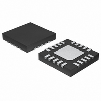
MAX3272AETP+ Maxim Integrated Products, MAX3272AETP+ Datasheet

MAX3272AETP+
Specifications of MAX3272AETP+
Related parts for MAX3272AETP+
MAX3272AETP+ Summary of contents
Page 1
... Selectable Output Polarity ✕ 4mm QFN pack- PART Applications MAX3272EGP MAX3272E/D MAX3272AETP+ -40°C to +85°C MAX3272AEGP + Denotes Lead-Free Package. *Dice are designed and guaranteed to operate from -40°C to +85°C, but are tested only at T Pin Configuration appears at end of data sheet ...
Page 2
Low-Power Limiting Amplifiers ABSOLUTE MAXIMUM RATINGS Power-Supply Voltage (V ) .................................-0.5V to +6.0V CC Voltage at IN+, IN- ..........................(V CC Voltage at SQUELCH, CAZ1, CAZ2, TH, CLOS ...............................................-0. LOS (MAX3272)...........................-0.5V to +6.0V Voltage at LOS, Voltage ...
Page 3
ELECTRICAL CHARACTERISTICS (continued +3.0V to +3.6V -40°C to +85°C. Typical values are PARAMETER SYMBOL High LOS Deassert Level LOS Output High Voltage LOS Output Low Voltage Squelch Input Current Note 1: Dice ...
Page 4
Low-Power Limiting Amplifiers (V = +3.3V +25°C, unless otherwise noted RANDOM JITTER vs. INPUT AMPLITUDE 100 1000 10,000 INPUT AMPLITUDE (mV ...
Page 5
T = +25°C, unless otherwise noted COMMON-MODE REJECTION RATIO 19.0 18.5 18.0 17.5 17.0 16.5 16.0 15.5 15.0 100k PIN NAME GND Supply Ground 2 IN+ Noninverted Input Signal 3 IN- Inverted ...
Page 6
Low-Power Limiting Amplifiers 50Ω 50Ω CONTROL MAX3272/ MAX3272A R TH CML SUPPLY CURRENT ( Figure 1. Power-Supply Current Measurement MAX3272/ MAX3272A IN+ CML 100Ω INPUT BUFFER IN- OFFSET CORRECTION Figure 2. Functional ...
Page 7
V CC 540Ω 0.25pF IN+ 110Ω IN- 0.25pF ESD STRUCTURES GND Figure 3. Input Circuit Two control voltages V , and V ASSERT the LOS assert and deassert levels. To prevent LOS chatter in the region of the programmed threshold, ...
Page 8
Low-Power Limiting Amplifiers V CC 50Ω 50Ω GND LEVEL Figure 5. CML Output Circuit CML Output Buffer The MAX3272/MAX3272A CML output circuit (Figure 5) provides high tolerance to impedance mismatches and inductive connectors. The output current can be ...
Page 9
Pin Configuration TOP VIEW GND 1 IN+ 2 IN- 3 MAX3272/ GND 4 MAX3272A QFN* NOTE: EXPOSED PAD MUST BE CONNECTED TO SUPPLY GROUND ...
Page 10
Low-Power Limiting Amplifiers +3.3V MAX3271 *THE MAX3202E PROVIDES ESD PROTECTION ON THE LOS PIN Wire Bonding Die For high-current density and reliable operation, the MAX3272 uses gold metallization. Make connections to the dice with gold wire only, and ...
Page 11
V CC (PAD 21) GND (PAD 1) IN+ (PAD 2) IN- (PAD 3) GND (PAD 4) TH (PAD (PAD 6) TRANSISTOR COUNT: 726 PROCESS: SiGe Bipolar SUBSTRATE: Insulator, Connect to GND DIE SIZE: 1.68mm ✕ 1.57mm DIE ...
Page 12
Low-Power Limiting Amplifiers (The package drawing(s) in this data sheet may not reflect the most current specifications. For the latest package outline information www.maxim-ic.com/packages.) 12 ______________________________________________________________________________________ Package Information PACKAGE OUTLINE 12,16,20,24L QFN, 4x4x0. 21-0106 ...
Page 13
For the latest package outline information www.maxim-ic.com/packages.) ______________________________________________________________________________________ +3.3V, 2.5Gbps Low-Power Limiting Amplifiers Package Information (continued) PACKAGE OUTLINE 12,16,20,24L QFN, 4x4x0. 21-0106 ...
Page 14
... Maxim cannot assume responsibility for use of any circuitry other than circuitry entirely embodied in a Maxim product. No circuit patent licenses are implied. Maxim reserves the right to change the circuitry and specifications without notice at any time. 14 ____________________Maxim Integrated Products, 120 San Gabriel Drive, Sunnyvale, CA 94086 408-737-7600 © 2004 Maxim Integrated Products Package Information (continued) Printed USA is a registered trademark of Maxim Integrated Products ...


