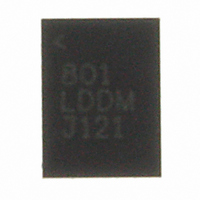
LTC6420CUDC-20#PBF Linear Technology, LTC6420CUDC-20#PBF Datasheet

LTC6420CUDC-20#PBF
Specifications of LTC6420CUDC-20#PBF
Available stocks
Related parts for LTC6420CUDC-20#PBF
LTC6420CUDC-20#PBF Summary of contents
Page 1
... The LTC6420-20 is packaged in a compact 20-lead 3mm × 4mm QFN package and operates over the –40°C to 85°C temperature range. L, LT, LTC, LTM, Linear Technology and the Linear logo are registered trademarks of Linear Technology Corporation. All other trademarks are the property of their respective owners. +OUT A ...
Page 2
... Output Short Circuit Duration........................... Indefi nite ORDER INFORMATION LEAD FREE FINISH TAPE AND REEL LTC6420CUDC-20#PBF LTC6420CUDC-20#TRPBF LDDM LTC6420IUDC-20#PBF LTC6420IUDC-20#TRPBF Consult LTC Marketing for parts specifi ed with wider operating temperature ranges. *The temperature grade is identifi label on the shipping container. ...
Page 3
DC ELECTRICAL CHARACTERISTICS temperature range, otherwise specifi cations are at T otherwise noted. SYMBOL PARAMETER Input/Output Characteristic G Gain DIFF ΔG Gain Matching TC Gain Temperature Drift GAIN V Output Swing Low (V = 1.5V) SWINGMIN OCM V Output Swing ...
Page 4
LTC6420-20 AC ELECTRICAL CHARACTERISTICS temperature range, otherwise specifi cations are at T SYMBOL PARAMETER ΔG Gain Matching ΔP Phase Matching Channel Separation (Note 8) –3dBBW –3dB Bandwidth 0.5dBBW Bandwidth for 0.5dB Flatness 0.1dBBW Bandwidth for 0.1dB Flatness NF Noise Figure ...
Page 5
TYPICAL PERFORMANCE CHARACTERISTICS Channel to Channel Gain Match vs Frequency 0.5 0.4 0.3 0.2 0.1 0.0 –0.1 –0.2 –0.3 –0.4 –0.5 10 100 1000 2000 FREQUENCY (MHz) 642020 G01 Frequency Response 100 FREQUENCY ...
Page 6
LTC6420-20 TYPICAL PERFORMANCE CHARACTERISTICS Noise Figure and Input Referred Noise Voltage vs Frequency NOISE FIGURE 100 1000 FREQUENCY (MHz) 642020 G08 ...
Page 7
PIN FUNCTIONS +INA, –INA, –INB, +INB (Pins 6): Differential Inputs of A and B channel respectively. – V (Pins 3, 4, 13, 14, 21): Negative Power Supply. All four pins, as well as the exposed back, must ...
Page 8
LTC6420-20 APPLICATIONS INFORMATION Circuit Operation Each of the two channels of the LTC6420-20 is composed of a fully differential amplifi er with on chip feedback and output common mode voltage control circuitry. Differential gain and input impedance are set by ...
Page 9
APPLICATIONS INFORMATION matching network while the other input is connected to the same matching network and a source resistor. Because the return ratios of the two feedback paths are equal, the two outputs have the same gain and thus symmetrical ...
Page 10
... C39 C32 [1] C32 J6 0.1μF 0.1μ 1000pF –OUTB R12 2 R14 88.7 [1] C40 1 5 0.1μF J8 TCM4-19+ R15 1 2 +OUTB C44 88.7 C41 0.1μF [1] VERSION U1 R5, R9, R10, R13 T1, T3 –C LTC6420CUDC-20 NONE TCM4-19+ –G LTC6421CUDC-20 NONE TCM4-19+ 642020 F04b 642020fb ...
Page 11
TYPICAL APPLICATIONS PORT 1 (50Ω) 1/2 AGILENT E5071C PORT 2 (50Ω) + – Test Circuit B, 4-Port Measurements (Only the Signal-Path Connections Are Shown) 0.1μ 1000Ω G OUT +INA +OUTA 100Ω 12.5Ω + – – + ...
Page 12
LTC6420-20 PACKAGE DESCRIPTION 3.50 ± 0.05 2.10 ± 0.05 2.65 ± 0.05 1.50 REF 1.65 ± 0.05 0.25 ±0.05 0.50 BSC 2.50 REF 3.10 ± 0.05 4.50 ± 0.05 RECOMMENDED SOLDER PAD PITCH AND DIMENSIONS APPLY SOLDER MASK TO AREAS ...
Page 13
... Changes to Applications Changes to Related Parts Information furnished by Linear Technology Corporation is believed to be accurate and reliable. However, no responsibility is assumed for its use. Linear Technology Corporation makes no representa- tion that the interconnection of its circuits as described herein will not infringe on existing patent rights. LTC6420-20 ...
Page 14
... Single Amplifi er per IC, High V Performance A = 8dB, 14dB, 20dB, 26dB; Single Amplifi er per IC, Low Power V 1.6nV/√Hz Noise, –72dBc Distortion at 50MHz, 18mA www.linear.com ● 0.1μF 1/2 LTC2285 V CM 642020 TA04 = 1, – 0310 REV B • PRINTED IN USA LINEAR TECHNOLOGY CORPORATION 2008 642020fb ...


