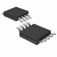
LT1567IMS8#PBF Linear Technology, LT1567IMS8#PBF Datasheet - Page 6

LT1567IMS8#PBF
Manufacturer Part Number
LT1567IMS8#PBF
Description
IC BLOCK BUILD FLTR LONOIS 8MSOP
Manufacturer
Linear Technology
Type
General Purposer
Datasheet
1.LT1567CMS8.pdf
(16 pages)
Specifications of LT1567IMS8#PBF
Applications
Filter
Mounting Type
Surface Mount
Package / Case
8-MSOP, Micro8™, 8-uMAX, 8-uSOP,
Lead Free Status / RoHS Status
Lead free / RoHS Compliant
LT1567
PI FU CTIO S
OAOUT (Pin 1): Output of the Uncommitted Op Amp (OA).
As with most wideband op amps, it is important to avoid
connecting heavy capacitive loads (above about 10pF)
directly to this output. Such loads will impair AC stability
and should be isolated from the output through series
resistance.
OAIN (Pin 2): Inverting or “–” Input of the Uncommitted
Op Amp (OA) in the LT1567. The noninverting or “+” input
of this amplifier is shared with that of the INV amplifier and
accessed via the DC BIAS and BYPASS pins. The OA
amplifier is optimized for minimal wideband noise.
BYPASS (Pin 3): AC Ground Bypass. A decoupling capaci-
tor, typically 0.1µF, from this pin to a printed circuit ground
plane must be used. Use the shortest possible wiring.
Power Supply Pins (Pins 4, 8): The V
be bypassed with 0.1µF capacitors to an adequate analog
ground plane using the shortest possible wiring. Electri-
cally clean supplies and a low impedance ground are
important to obtain the wide dynamic range and band-
width available from the LT1567. Low noise linear power
supplies are recommended. Switching supplies require
special care because of the inevitable risk of their switch-
ing noise coupling into the signal path, reducing dynamic
range.
6
U
U
U
–
and V
+
pins should
DC BIAS (Pin 5): DC Biasing Input. Sets the DC voltage at
the noninverting inputs of the two internal amplifiers;
designed for use as a DC reference, not a signal input.The
DC BIAS input includes a small series resistor, both to
balance DC offsets in the presence of input bias currents
and also to suppress the “Q” factor of possible parasitic
high frequency resonant circuits introduced by wiring
inductance. The reference voltage at the noninverting
inputs of the two amplifiers is decoupled for very high
frequencies with a small internal capacitor to the chip
substrate, nominally 7pF. An external capacitor, typically
0.1µF, to a nearby ground plane must be added at Pin 3
(BYPASS) for a clean wideband DC reference biasing
voltage.
INVIN (Pin 6): Unity-Gain Inverter Input. The “inverter”
(INV) amplifier in the LT1567 is connected to internal
resistors (nominally 600Ω each) to form a closed-loop
amplifier with a wideband voltage gain of nominally –1.
This amplifier is similar to the uncommitted op amp (OA)
but is optimized for high frequency linearity.
INVOUT (Pin 7): Output of the INV or “Inverter” Amplifier,
with a Nominal Gain of –1 from the INVIN Pin. As with
most wideband op amps, it is important to avoid connect-
ing heavy capacitive loads (above about 10pF) directly to
this output. Such loads will impair AC stability and should
be isolated from the output through series resistance.
1567fa


