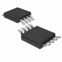
LT1567IMS8#TRPBF Linear Technology, LT1567IMS8#TRPBF Datasheet - Page 12

LT1567IMS8#TRPBF
Manufacturer Part Number
LT1567IMS8#TRPBF
Description
IC BLOCK BUILD FLTR LONOIS 8MSOP
Manufacturer
Linear Technology
Type
General Purposer
Datasheet
1.LT1567CMS8.pdf
(16 pages)
Specifications of LT1567IMS8#TRPBF
Applications
Filter
Mounting Type
Surface Mount
Package / Case
8-MSOP, Micro8™, 8-uMAX, 8-uSOP,
Lead Free Status / RoHS Status
Lead free / RoHS Compliant
LT1567
APPLICATIO S I FOR ATIO
Figure 4 shows an LT1567 single supply differential buffer
driving a differential 1st order RC filter. The V
is subject to the common mode (DC BIAS) limits in the
spec table. Within this constraint, V
adjust the output common mode level, as noted in Figure
4. For example, in a single 5V power supply circuit, if the
input common mode DC voltage is 1.1V and V
then the output common mode DC voltage is 2.5V.
Figure 5 shows a low noise differential to single ended
amplifier and 1st order lowpass filter. The input common
mode rejection depends on the matching of resistors R1
and R3 and the LT1567 inverter gain tolerance (common
mode rejection is at least 38dB up to 1MHz with 1%
resistors and 5% inverter gain tolerance). The DC voltage
at the amplifier’s output (V
12
U
V
V
V
REF
IN1
IN2
U
OUT
604Ω
0.1µF
) is V
3
5
2
W
REF
LT1567
REF
V
V
COMMON MODE V
V
f
ηBW
.
OUT1
OUT2
DIFF
604Ω
can be used to
–
+
IS THE NOISE BANDWIDTH
= V
150Ω
= –V
= –V
Figure 4. A Differential Buffer/Driver
OUT2
IN2
IN1
8
REF
REF
V
V
U
+
+
– V
+ 2V
+ 2V
0.1µF
is 1.8V,
OUT1
voltage
OUT
REF
REF
7pF
IS 2V
= V
1
IN2
REF
6
– V
600Ω
– (COMMON MODE V
–
+
IN1
Output Drive
The output of the LT1567 op amp (Pin 1) can typically
provide at least ±20mA. The minimum resistive load to
ground that Pin 1 or Pin 7 can drive depends on the
feedback resistor and the peak output voltage. For ex-
ample, the differential driver circuit in Figure 4 is operating
with a single 5V supply, V
and the peak AC signal (V
1.66mA to the feedback resistors (1V/604Ω), then 18.34mA
is available to drive a resistive load. With the peak output
voltage at 3.5V (2.5V DC plus 1V peak AC), the outputs can
drive resistive loads of 191Ω or greater.
f
f
600Ω
ηBW
–3dB
4
V
–
=
=
4π • R • C
4π • R • C
1.57
1
IN
)
1567 F04a
7
V
V
OUT1
OUT2
R
R
INAC
REF
) is 1V. If the outputs provide
C
and V
V
DIFF
INDC
are equal to 2.5V
1567fa


