PA09A Cirrus Logic Inc, PA09A Datasheet - Page 4
PA09A
Manufacturer Part Number
PA09A
Description
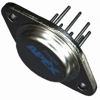
OP AMP VID 80V 5A TO-3-8 CE SG
Manufacturer
Cirrus Logic Inc
Series
Apex Precision Power™r
Specifications of PA09A
Applications
General Purpose
Number Of Circuits
1
Slew Rate
220 V/µs
Current - Supply
70mA
Current - Output / Channel
4.5A
Voltage - Supply, Single/dual (±)
24 V ~ 80 V, ±12 V ~ 40 V
Mounting Type
Surface Mount
Package / Case
TO-3-8
Number Of Channels
1
Voltage Gain Db
98 dB
Common Mode Rejection Ratio (min)
104 dB
Input Offset Voltage
0.5 mV
Maximum Operating Temperature
+ 85 C
Mounting Style
Through Hole
Maximum Dual Supply Voltage
+/- 40 V
Minimum Operating Temperature
- 25 C
Lead Free Status / RoHS Status
Lead free / RoHS Compliant
Other names
598-1299
Available stocks
Company
Part Number
Manufacturer
Quantity
Price
Company:

Part Number:
PA09A
Manufacturer:
Cirrus Logic Inc
Quantity:
135
Part Number:
PA09A
Manufacturer:
APEX
Quantity:
20 000


PA09 • PA09A
GENERAL
siderations" which covers stability, supplies, heat sinking,
mounting, current limit, SOA interpretation, and specification
interpretation. visit www.Cirrus.com for design tools that help
automate tasks such as calculations for stability, internal power
dissipation, current limit; heat sink selection; Apex Precision
Power’s complete Application Notes library; Technical Seminar
workbook; and Evaluation Kits.
SUPPLY VOLTAGE
having equal voltages. A nonsymmetrical (ie. +70/–10v) or a
single supply (ie. 80v) may be used as long as the total volt-
age between the +v
of the voltages of the specified dual supply.
SAFE OPERATING AREA (SOA)
fier has two distinct limitations:
1. The current handling capability of the MOSFET geometry
2. The junction temperature of the output MOSFETs.
SAFE OPERATING AREA CURVES
for internal thermal delays. For a given application, the direc-
tion and magnitude of the output current should be calculated
or measured and checked against the SOA curves. This is
simple for resistive loads but more complex for reactive and
EMF generating loads. The following guidelines may save
extensive analytical efforts:
1. Capacitive and inductive loads up to the following maximums
4
Please read Application Note 1 "General Operating Con-
The specified voltage (±v
The MOSFET output stage of this power operational ampli-
The SOA curves combine the effect of these limits and allow
and the wire bonds.
are safe:
2.0
5.0
4.0
3.5
3.0
2.5
1.5
INTERNAL VOLTAGE DROP SUPPLY TO OUTPUT V
40v
30v
20v
±V
15v
S
CAPACITIVE LOAD
15
S
2500µF
500µF
and –v
.1µF
20
∞
S
S
25
) applies for a dual (±) supply
SOA
rails does not exceed the sum
30
35
INDUCTIVE LOAD
40
100mH
24mH
75mH
11mH
50
T
C
60 70
S
= 25°C
–V
O
(V)
80
P r o d u c t I n n o v a t i o n F r o m
2. Short circuits to ground are safe with dual supplies up to
3. The output stage is protected against transient flyback.
BYPASSING OF SUPPLIES
lum capacitor of at least 47µF in parallel with a .47µF ceramic
capacitor directly connected from the power supply pins to the
ground plane.
OUTPUT LEADS
frequency range, even a few inches of wire have significant
inductance, raising the interconnection impedance and limit-
ing the output current slew rate. Furthermore, the skin effect
increases the resistance of heavy wires at high frequencies.
Multistrand litz wire is recommended to carry large video
currents with low losses.
GROUNDING
signal to a common ground plane will prevent undesired cur-
rent feedback, which can cause large errors and/or instabilities.
"Single point" is a key phrase here; a ground plane should be
used as shielding rather than a current path. leaving the case
of the PA09 floating will cause oscillations in some applications.
COMPENSATION
sation capacitor for any given gain. The most common ranges
are shown in the COMPENSATiON typical performance graph.
Swinging closer to the supply rails, heavier loads, faster input
signal rise and fall times and higher supply voltages all tend to
demand larger values of compensation capacitor. This capaci-
tor must be rated at least as high as the total voltage applied
to the amplifier. in making specific value choices, use the
square wave stability test presented in APPliCATiON NOTE
19, Figures 40 and 41.
step functions in the input signal, use this circuit to measure
large signal response. By increasing square wave amplitude to
the maximum of the application, this test may show significant
distortion of the output waveform following the square wave
transitions. in this case the faster input stages of the PA09
are out-running the output stage and overload recovery time
creates the distortion. This speed relationship is also why
slew rate does not increase for compensation values below
about 27pF.
SUPPLY CURRENT
demands extra supply current. The following graphs illustrate
this current for several conditions for both sine and square
wave signals. Current is exclusive of any load current and will
affect both supply rating and thermal ratings. when calculat-
ing internal power dissipation, multiply this current times total
supply voltage.
Each supply rail must be bypassed to common with a tanta-
Keep the output leads as short as possible. in the video
Single point grounding of the input resistors and the input
The PA09 is extremely flexible in terms of choice of compen-
in addition to small signal testing, if the application includes
when swinging large signals, the output stage of the PA09
Note that swinging closer to the supply rail demands more
±20v.
However, for protection against sustained, high energy
flyback, external fast-recovery diodes should be used.
PA09U
Related parts for PA09A
Image
Part Number
Description
Manufacturer
Datasheet
Request
R

Part Number:
Description:
IC PWR AMP 80V 5A 8PIN TO3
Manufacturer:
Cirrus Logic Inc
Datasheet:

Part Number:
Description:
Development Kit
Manufacturer:
Cirrus Logic Inc
Datasheet:
Part Number:
Description:
Development Kit
Manufacturer:
Cirrus Logic Inc
Datasheet:


Part Number:
Description:
High-efficiency PFC + Fluorescent Lamp Driver Reference Design
Manufacturer:
Cirrus Logic Inc
Datasheet:
Part Number:
Description:
Development Kit
Manufacturer:
Cirrus Logic Inc
Datasheet:
Part Number:
Description:
Development Kit
Manufacturer:
Cirrus Logic Inc
Datasheet:

Part Number:
Description:
Development Kit
Manufacturer:
Cirrus Logic Inc
Datasheet:
Part Number:
Description:
Development Kit
Manufacturer:
Cirrus Logic Inc
Datasheet:
Part Number:
Description:
Development Kit
Manufacturer:
Cirrus Logic Inc
Datasheet:

Part Number:
Description:
EVALUATION BOARD FOR CS8427
Manufacturer:
Cirrus Logic Inc
Datasheet:

Part Number:
Description:
BOARD EVAL FOR CS8416 RCVR
Manufacturer:
Cirrus Logic Inc
Datasheet:

Part Number:
Description:
EVALUATION BOARD FOR CS8420
Manufacturer:
Cirrus Logic Inc
Datasheet:

Part Number:
Description:
KIT DEVELOPMENT EP9315 ARM9
Manufacturer:
Cirrus Logic Inc
Datasheet:

Part Number:
Description:
KIT DEVELOPMENT EP9302 ARM9
Manufacturer:
Cirrus Logic Inc
Datasheet: