LT6551CMS#TRPBF Linear Technology, LT6551CMS#TRPBF Datasheet - Page 11

LT6551CMS#TRPBF
Manufacturer Part Number
LT6551CMS#TRPBF
Description
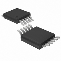
IC AMP VIDEO QUAD 3.3V 10-MSOP
Manufacturer
Linear Technology
Datasheet
1.LT6550CMS.pdf
(16 pages)
Specifications of LT6551CMS#TRPBF
Applications
Voltage Feedback
Output Type
Rail-to-Rail
Number Of Circuits
4
-3db Bandwidth
90MHz
Slew Rate
600 V/µs
Current - Supply
8.5mA
Current - Output / Channel
60mA
Voltage - Supply, Single/dual (±)
3 V ~ 12.6 V
Mounting Type
Surface Mount
Package / Case
10-TFSOP, 10-MSOP (0.118", 3.00mm Width)
Lead Free Status / RoHS Status
Lead free / RoHS Compliant
Available stocks
Company
Part Number
Manufacturer
Quantity
Price
Amplifier Characteristics
Figure 1 shows a simplified schematic of one channel of
the LT6551 quad. Resistors RF and RG provide an internal
gain of 2. (The LT6550 triple is a slight variation with the
gain setting resistor, RG, connected to a separate ground
pin). The input stage consists of transistors Q1 to Q8 and
resistor R1. This topology allows for high slew rates at low
supply voltages. There are back-to-back series diodes, D1
to D4, across the + and – inputs of each amplifier to limit
the differential input voltage to ±1.4V. R
current through these diodes if the input differential volt-
age exceeds ±1.4V. The input stage drives the degenera-
tion resistors of PNP and NPN current mirrors, Q9 to Q12,
that convert the differential signals into a single-ended
output. The complementary drive generator supplies cur-
rent to the output transistors that swing from rail-to-rail.
Input Voltage Range
The input voltage range is V
temperature. If the device is operated on a single 3V supply
APPLICATIO S I FOR ATIO
DESD1
IN
DESD2
GND
V
+
225Ω
R
U
IN
D1
D2
RG
450Ω
U
450Ω
RF
EE
+
D3
D4
to (V
W
Q2
Q1
I1
CC
– 1.75V) over
Figure 1. LT6551 Simplified Schematic
Q3
Q4
IN
R1
limits the
U
Q5
Q6
Q7
Q8
I2
–
the maximum input is (3V – 1.75V) or 1.25V, and the
internal gain of two will set the output voltage to 2.5V.
Increasing the input beyond 1.25V will force the device out
of its linear range, no longer a gain of 2, and the output will
not increase beyond 2.5V. At a higher supply voltage, i.e.
5V, the maximum input voltage is 5V – 1.75V or 3.25V.
However, due to the internal gain of 2, the output will clip
with a lower input voltage. For linear unclipped operation
the minimum input voltage is (V
mum input voltage is (V
whichever is less.
ESD
The LT6550/LT6551 have reverse-biased ESD protection
diodes on all inputs and outputs as shown in Figure 1. If
these pins are forced beyond either supply, unlimited
current will flow through these diodes. If the current is
limited to 10mA or less, no damage to the device will
occur.
I3
I4
Q11
Q9
R2
R4
Q10
Q12
R3
R5
COMPLEMENTARY
GENERATOR
DRIVE
OUT
CM
LT6550/LT6551
Max)/2 or (V
Q13
Q14
OUT
Min)/2 and the maxi-
GND
V
+
DESD3
DESD4
CC
6551 F01
V
OUT
GND
+
– 1.75V),
11
65501fa


