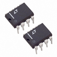
LT1193CN8 Linear Technology, LT1193CN8 Datasheet - Page 8

LT1193CN8
Manufacturer Part Number
LT1193CN8
Description
IC AMP VIDEO DIF ADJ GAIN 8-DIP
Manufacturer
Linear Technology
Datasheet
1.LT1193CN8PBF.pdf
(12 pages)
Specifications of LT1193CN8
Applications
Differential
Number Of Circuits
1
-3db Bandwidth
80MHz
Slew Rate
500 V/µs
Current - Supply
35mA
Current - Output / Channel
50mA
Voltage - Supply, Single/dual (±)
4.75 V ~ 16 V, ±2.38 V ~ 8 V
Mounting Type
Through Hole
Package / Case
8-DIP (0.300", 7.62mm)
Lead Free Status / RoHS Status
Contains lead / RoHS non-compliant
Available stocks
Company
Part Number
Manufacturer
Quantity
Price
Company:
Part Number:
LT1193CN8
Manufacturer:
LT
Quantity:
5 510
Part Number:
LT1193CN8#PBF
Manufacturer:
LINEAR/凌特
Quantity:
20 000
V
APPLICATIO S I FOR ATIO
LT1193
In many applications and those requiring good settling
time it is important to use multiple bypass capacitors. A
0.1 F ceramic disc in parallel with a 4.7 F tantalum is
recommended. Two oscilloscope photos with different
bypass conditions are used to illustrate the settling time
characteristics of the amplifier. Note that although the
output waveform looks acceptable at 1V/DIV, when ampli-
fied to 10mV/DIV the settling time to 10mV is 347ns for the
0.1 F bypass; the time drops to 96ns with multiple bypass
capacitors.
8
INDIFF
V
IN
V
IN
3
2
1
8
3
2
1
8
R
R
G
G
SHDN
SHDN
V
+
–
–/FB
+
–
–/FB
+/REF
+/REF
O
LT1193
LT1193
A
= (V
5
5
V
V
V
R
V
V
= +
R
FB
INDIFF
+
–
+
–
FB
7
4
7
4
R
FB
No Supply Bypass Capacitors
R
+ V
+ R
G
A
6
6
IN
V
U
G
= 10, IN DEMO BOARD, R
)
R
FB
V
V
R
OUT
OUT
+ R
G
U
G
V
IN
V
R
INDIFF
G
V
V
O
IN
=
W
(
L
R
= 1k
3
2
1
8
FB
R
3
2
1
8
G
R
SHDN
+
–
+ R
+/REF
–/FB
G
SHDN
+
–
–/FB
+/REF
LT1193
LT1193
A
G
5
5
V
(
R
V
V
V
= –
R
V
V
LT1192 • TA04
FB
+
–
INDIFF
7
4
FB
+
7
4
–
R
FB
U
R
–
+ R
G
( (
6
6
R
R
LT1193 • TA03
G
FB
G
V
V
V
IN
OUT
OUT
Operating With Low Closed-Loop Gains
The LT1193 has been optimized for closed-loop gains of
2 or greater; the frequency response illustrates the ob-
tainable closed-loop bandwidths. For a closed-loop gain
of 2 the response peaks about 2dB. Peaking can be
minimized by keeping the feedback elements below 1k ,
and can be eliminated by placing a capacitor across the
feedback resistor, (feedback zero). This peaking shows
up as time domain overshoot of about 40%. With the
feedback capacitor it is eliminated.
Cable Terminations
The LT1193 video difference amplifier has been optimized
as a low cost cable driver. The 50mA guaranteed output
current enables the LT1193 to easily deliver 7.5V
1V/DIV
1V/DIV
V
V
OUT
OUT
0V
0V
SUPPLY BYPASS CAPACITORS = 0.1 F + 4.7 F TANTALUM
SUPPLY BYPASS CAPACITORS = 0.1 F
Settling Time Good Bypass
Settling Time Poor Bypass
SETTLING TIME TO 10mV, A
SETTLING TIME TO 10mV, A
V
V
= 2
= 2
LT1192 • TA05
LT1192 • TA06
0V
0V
P-P
V
10mV/DIV
V
10mV/DIV
OUT
OUT
1193fb
into


