AD534JH Analog Devices Inc, AD534JH Datasheet

IC MULT DIV LASER TRIM TO100-10

AD534JH

Manufacturer Part Number
AD534JH
Description
IC MULT DIV LASER TRIM TO100-10
Manufacturer
Analog Devices Inc
Datasheets

Specifications of AD534JH

Rohs Status
RoHS non-compliant
Function
Analog Multiplier/Divider
Number Of Bits/stages
4-Quadrant
Package / Case
TO-100, Metal Can (10 Leads)
No. Of Multipliers / Dividers
1
No. Of Amplifiers
1
Supply Voltage Range
± 8V To ± 18V
Slew Rate
20V/µs
Operating Temperature Range
0°C To +70°C
Digital Ic Case Style
TO-100
No. Of Pins
10
Lead Free Status / RoHS Status
Contains lead / RoHS non-compliant

Available stocks

Company
Part Number
Manufacturer
Quantity
Price
Part Number:
AD534JH
Manufacturer:
ADI
Quantity:
632
Part Number:
AD534JH
Manufacturer:
ADI/亚德诺
Quantity:
20 000
Part Number:
AD534JHZ
Manufacturer:
ADI
Quantity:
632
a
PRODUCT DESCRIPTION
The AD534 is a monolithic laser trimmed four-quadrant multi-
plier divider having accuracy specifications previously found
only in expensive hybrid or modular products. A maximum
multiplication error of 0.25% is guaranteed for the AD534L
without any external trimming. Excellent supply rejection, low
temperature coefficients and long term stability of the on-chip
thin film resistors and buried Zener reference preserve accuracy
even under adverse conditions of use. It is the first multiplier to
offer fully differential, high impedance operation on all inputs,
including the Z-input, a feature which greatly increases its flex-
ibility and ease of use. The scale factor is pretrimmed to the
standard value of 10.00 V; by means of an external resistor, this
can be reduced to values as low as 3 V.
The wide spectrum of applications and the availability of several
grades commend this multiplier as the first choice for all new
designs. The AD534J ( 1% max error), AD534K ( 0.5% max)
and AD534L ( 0.25% max) are specified for operation over the
0 C to +70 C temperature range. The AD534S ( 1% max) and
AD534T ( 0.5% max) are specified over the extended tempera-
ture range, –55 C to +125 C. All grades are available in her-
metically sealed TO-100 metal cans and TO-116 ceramic DIP
packages. AD534J, K, S and T chips are also available.
PROVIDES GAIN WITH LOW NOISE
The AD534 is the first general purpose multiplier capable of
providing gains up to X100, frequently eliminating the need for
separate instrumentation amplifiers to precondition the inputs.
The AD534 can be very effectively employed as a variable gain
differential input amplifier with high common-mode rejection.
The gain option is available in all modes, and will be found to
simplify the implementation of many function-fitting algorithms
REV. B
Information furnished by Analog Devices is believed to be accurate and
reliable. However, no responsibility is assumed by Analog Devices for its
use, nor for any infringements of patents or other rights of third parties
which may result from its use. No license is granted by implication or
otherwise under any patent or patent rights of Analog Devices.
FEATURES
Pretrimmed to
All Inputs (X, Y and Z) Differential, High Impedance for
Scale-Factor Adjustable to Provide up to X100 Gain
Low Noise Design: 90 V rms, 10 Hz–10 kHz
Low Cost, Monolithic Construction
Excellent Long Term Stability
APPLICATIONS
High Quality Analog Signal Processing
Differential Ratio and Percentage Computations
Algebraic and Trigonometric Function Synthesis
Wideband, High-Crest rms-to-dc Conversion
Accurate Voltage Controlled Oscillators and Filters
Available in Chip Form
[(X
1
– X
2
) (Y
1
– Y
0.25% max 4-Quadrant Error (AD534L)
2
)/10 V] + Z
2
Transfer Function
One Technology Way, P.O. Box 9106, Norwood, MA 02062-9106, U.S.A.
Tel: 781/329-4700
Fax: 781/326-8703
such as those used to generate sine and tangent. The utility of
this feature is enhanced by the inherent low noise of the AD534:
90 V, rms (depending on the gain), a factor of 10 lower than
previous monolithic multipliers. Drift and feedthrough are also
substantially reduced over earlier designs.
UNPRECEDENTED FLEXIBILITY
The precise calibration and differential Z-input provide a degree
of flexibility found in no other currently available multiplier.
Standard MDSSR functions (multiplication, division, squaring,
square-rooting) are easily implemented while the restriction to
particular input/output polarities imposed by earlier designs has
been eliminated. Signals may be summed into the output, with
or without gain and with either a positive or negative sense.
Many new modes based on implicit-function synthesis have
been made possible, usually requiring only external passive
components. The output can be in the form of a current, if
desired, facilitating such operations as integration.
SF
Y1
TO-100 (H-10A)
X2
Y2
(Not To Scale)
Package
TOP VIEW
AD534
–V
X1
NC
NC
NC
NC
S
SF
NC = NO CONNECT
PIN CONFIGURATIONS
4
5
6
7
8
Precision IC Multiplier
World Wide Web Site: http://www.analog.com
+V
Z2
S
3
9
OUT
Z1
LCC (E-20A)
Internally Trimmed
(Not To Scale)
10
TOP VIEW
2
Package
AD534
11 12 13
1
20 19
© Analog Devices, Inc., 1999
NC
NC
X1
X2
SF
Y1
Y2
TO-116 (D-14)
NC = NO CONNECT
1
2
3
4
5
6
7
18
17
16
15
14
(Not to Scale)
Package
TOP VIEW
OUT
NC
Z1
NC
Z2
AD534
AD534
14
13
12
11
10
9
8
+V
NC
OUT
Z1
Z2
NC
–V
S
S

Related parts for AD534JH

AD534JH Summary of contents

Page 1

FEATURES Pretrimmed to 0.25% max 4-Quadrant Error (AD534L) All Inputs (X, Y and Z) Differential, High Impedance for [(X – – Scale-Factor Adjustable to Provide up ...

Page 2

... AD534JH AD534KH AD534JD AD534KD AD534K Chips Specifications shown in boldface are tested on all production units at final electrical test. Results from those tests are used to calculate outgoing quality levels. All min and and SF. max specifications are guaranteed, although only those shown in boldface are tested S on all production units ...

Page 3

Model MULTIPLIER PERFORMANCE Transfer Function 1 Total Error (– + min to max A Total Error vs. Temperature Scale Factor Error 2 (SF = 10.000 V Nominal) Temperature-Coefficient of Scaling Voltage Supply Rejection ( ...

Page 4

... C haracteristics Thermal Resistance = 25 C/W for H-10A JC = 150 C/W for H-10A C/W for D-14 or E-20A C/W for D-14 or E-20A JA Model AD534JD AD534KD AD534LD AD534JH AD534JH/+ AD534KH AD534KH/+ AD534LH AD534K Chip AD534SD AD534SD/883B AD534TD AD534TD/883B JM38510/13902BCA JM38510/13901BCA AD534SE AD534SE/883B AD534TE/883B AD534SH AD534SH/883B ...

Page 5

FUNCTIONAL DESCRIPTION Figure functional block diagram of the AD534. Inputs are converted to differential currents by three identical voltage-to- current converters, each trimmed for zero offset. The product of the X and Y currents is generated by ...

Page 6

AD534 A much lower scaling voltage can be achieved without any re- duction of input signal range using a feedback attenuator as shown in Figure 4. In this example, the scale is such that V = XY, so that the ...

Page 7

OPERATION AS A DIVIDER The AD535, a pin-for-pin functional equivalent to the AD534, has guaranteed performance in the divider and square-rooter configurations and is recommended for such applications. Figure 6 shows the connection required for division. Unlike earlier products, the ...

Page 8

AD534–Applications Section The versatility of the AD534 allows the creative designer to implement a variety of circuits such as wattmeters, frequency doublers and automatic gain controls to name but a few +15V – B ...

Page 9

CONTROL INPUT, E 100mV TO 10V CALIBRATION PROCEDURE: WITH E TRIMMER CAPACITOR TO SET f = 8.000kHz. LINEARITY WILL TYPICALLY BE WITHIN DUE TO DELAYS IN THE COMPARATOR, THIS TECHNIQUE IS NOT SUITABLE FOR MAXIMUM FREQUENCIES ABOVE 10kHz. FOR FREQUENCIES ...

Page 10

AD534–Typical Performance Curves 14 OUTPUT ALL INPUTS 10V POSITIVE OR NEGATIVE SUPPLY – Volts Figure 16. Input/Output Signal Range vs. Supply Voltages 800 700 600 SCALING ...

Page 11

RMS 0pF L –10 C 1000pF –20 WITH X10 FEEDBACK ATTENUATOR –30 100k 10k FREQUENCY – Hz Figure 22. Frequency Response as a ...

Page 12

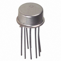
AD534 0.355 (9.02) 0.305 (7.75) 0.370 (9.40) 0.335 (8.51) 0.035 0.89 0.125 (3.18) MIN OUTLINE DIMENSIONS Dimensions shown in inches and (mm). H-10A Package TO-100 REFERENCE PLANE 0.562 (14.30) 0.115 (2.92) 0.185 (4.70) 0.500 (12.70) 0.165 (4.19 ...

Related keywords