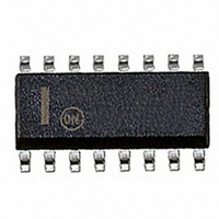
SA572DR2G ON Semiconductor, SA572DR2G Datasheet - Page 5

SA572DR2G
Manufacturer Part Number
SA572DR2G
Description
IC COMPANDOR 2CHAN GAIN 16-SOIC
Manufacturer
ON Semiconductor
Type
Compandorr
Datasheet
1.SA572DTBR2.pdf
(12 pages)
Specifications of SA572DR2G
Applications
Automatic Level Control, Stereo Expander
Mounting Type
Surface Mount
Package / Case
16-SOIC (0.300", 7.5mm Width)
Lead Free Status / RoHS Status
Lead free / RoHS Compliant
Other names
SA572DR2G
SA572DR2GOSTR
SA572DR2GOSTR
Available stocks
Company
Part Number
Manufacturer
Quantity
Price
is caused by gain control ripple. In a compandor system,
available control of fast attack and slow recovery improve
ripple distortion significantly. At the unity gain level of
100 mV, the gain cell gives THD (total harmonic
distortion) of 0.17% typ. Output noise with no input signals
Rectifier
The input voltage is converted to current through the input
resistor R
signal polarity. Deadband of the voltage to current
converter is reduced by the loop gain of the gain block A
If AC coupling is used, the rectifier error comes only from
input bias current of gain block A
is typically about 70 nA. Frequency response of the gain
block A
The collector current of Q
collector of Q
current I
to:
current I
band the input range of the rectifier is about 52 dB.
The residual distortion is third harmonic distortion and
The rectifier is a full-wave design as shown in Figure 4.
If V
The internal bias scheme limits the maximum output
IN
2
R
R
is AC-coupled, then the equation will be reduced
also causes second-order error at high frequency.
2
. The rectifier transfer function is:
to be around 300 mA. Within a "1.0 dB error
and turns on either Q
5
to form the full wave rectified output
I
I
R
RAC
+
+
I
6
V
O
is mirrored and summed at the
IN
V
* V
IN
R
Q
(AVG)
R
I
4
2
G
5
2
2
or Q
. The input bias current
REF
6
Q
3
depending on the
Figure 3. Basic Gain Cell Schematic
1
2
I
G
)
TRIM
THD
1
2
I
O
http://onsemi.com
(eq. 3)
2
.
+
5
A1
V
REF
is only 6.0 mV in the audio spectrum (10 Hz-20 kHz). The
output current I
operational amplifier with a resistor from output to
inverting input. The non-inverting input of the operational
amplifier has to be biased at V
is DC coupled.
V
−
V
REF
IN
140mA
6.8kW
Figure 4. Simplified Rectifier Schematic
I
R
1
1
V
R
IN
2
O
V+
must feed the virtual ground input of an
+
−
280mA
A2
Q
I
1
2
Q
2
REF
Q
Q
if the output current I
5
6
V+
I
R
D
+
7
V IN * V REF
R 2
O


