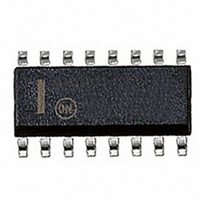
SA572DG ON Semiconductor, SA572DG Datasheet - Page 3

SA572DG
Manufacturer Part Number
SA572DG
Description
IC COMPANDOR 2CHAN GAIN 16-SOIC
Manufacturer
ON Semiconductor
Type
Compandorr
Datasheet
1.SA572DTBR2.pdf
(12 pages)
Specifications of SA572DG
Applications
Automatic Level Control, Stereo Expander
Mounting Type
Surface Mount
Package / Case
16-SOIC (0.300", 7.5mm Width)
Product
General Purpose Audio Amplifiers
Output Type
Programmable Analog
Available Set Gain
+/- 1.5 dB
Thd Plus Noise
0.2 %, 0.05 %, 0.25 %
Operating Supply Voltage
6 V to 22 V
Supply Current
6.3 mA
Maximum Power Dissipation
500 mW
Maximum Operating Temperature
+ 85 C
Mounting Style
SMD/SMT
Input Bias Current (max)
70 nA
Minimum Operating Temperature
- 40 C
Supply Voltage (max)
22 V
Supply Voltage (min)
6 V
Audio Control Type
Compandor
Output Power
500mW
Supply Voltage Range
6V To 22V
Operating Temperature Range
-40°C To +85°C
Audio Ic Case Style
SOIC
No. Of Pins
16
Logic Type
Comparator
Rohs Compliant
Yes
Operating Temperature (min)
-40C
Operating Temperature (max)
85C
Operating Temperature Classification
Industrial
Mounting
Surface Mount
Pin Count
16
Package Type
SOIC W
Leaded Process Compatible
Yes
Lead Free Status / RoHS Status
Lead free / RoHS Compliant
Stresses exceeding Maximum Ratings may damage the device. Maximum Ratings are stress ratings only. Functional operation above the
Recommended Operating Conditions is not implied. Extended exposure to stresses above the Recommended Operating Conditions may affect
device reliability.
MAXIMUM RATINGS
DC ELECTRICAL CHARACTERISTICS
signals at unity gain level (0 dB) = 100 mV
Supply Voltage
Operating Temperature Range
Operating Junction Temperature
Power Dissipation
Thermal Resistance, Junction−to−Ambient
Supply Voltage
Supply Current
Internal Voltage Reference
Total Harmonic Distortion (Untrimmed)
Total Harmonic Distortion (Trimmed)
Total Harmonic Distortion (Trimmed)
No Signal Output Noise
DC Level Shift (Untrimmed)
Unity Gain Level
Large-Signal Distortion
Tracking Error
(Measured relative to value at unity gain) =
[V
Channel Crosstalk
Power Supply Rejection Ratio
O
−V
V
2
O
V
1
(unity gain)] dB−V
C
C
R
A
2.2mF
= 10mF
= 1mF
2.2mF
Characteristic
3.3kW
1%
R
2
5W
(3,13)
(7,9)
2
dB
(2,14)
(4,12)
Rating
6.8kW
RECTIFIER
DG
RMS
BUFFER
Standard test conditions, V
at 1.0 kHz; V
Symbol
PSRR
THD
THD
THD
V
I
V
CC
CC
DTB Package
R
N Package
D Package
Figure 2. Test Circuit
http://onsemi.com
1
= V
V
V
grounded (20−20 kHz)
Input change from no
channel A, measured
1.0 kHz, C
signal to 100 mV
2
1.0 kHz, C
2
output on channel B
(8)
(1,15)
(16)
(6,10)
2
(5,11)
Input to V
V
= +6.0 dB, V
Test Conditions
= −30 dB, V
; R
200 mV
1
Rectifier Input
= V
2
3
No Signal
= 3.3 kW; R
100 Hz
120 Hz
1kW
2
= 400 mV
−
−
−
CC
RMS
82kW
A
R
1
Symbol
= 1.0 mF
and V
= 10 mF
= 15 V, T
1
R
1
V
into
P
T
T
= 0 dB
+
= 0 dB
qJA
CC
A
2.2k
J
D
RMS
3
2
= 17.3 kW, unless otherwise noted.
2.2mF
A
= 25°C; Expandor mode (see Test Circuit). Input
270pF
17.3kW
1%
R
3
−1.5
Min
6.0
2.3
60
−
−
−
−
−
−
−
−
−
−
+
−
0.1mF
NE5234
−40 to +85
1mF
Value
150
500
105
133
22
75
"0.2
"0.5
"20
0.05
0.25
Typ
2.5
0.2
6.0
0.7
70
−
−
0
−
+
+
22mF
22mF
−2.5, +1.6
100W
"50
Max
+1.5
6.3
2.7
1.0
3.0
22
25
−
−
−
−
+15V
V
0
°C/W
Unit
V
mW
°C
°C
DC
−15V
Unit
V
V
mA
mV
dB
dB
dB
dB
dB
mV
%
%
%
%
DC
DC


