DS2167QN/T&R Maxim Integrated Products, DS2167QN/T&R Datasheet
DS2167QN/T&R
Specifications of DS2167QN/T&R
Available stocks


Related parts for DS2167QN/T&R


DS2167QN/T&R Summary of contents
Page 1
FEATURES • Speech compression chip compatible with standard ADPCM algorithms: – DS2167 supports “new” T1Y1 recommenda- tions (July 1986) and “new” CCITT G.721 rec- ommendations – DS2168 supports “old” CCITT G.721 recom- mendations • Dual independent channel architecture – device ...
Page 2
DS2167/DS2168 PRODUCT OVERVIEW The DS2167 and DS2168 contain three major function- al blocks: a high performance (10 MIPS) DSP “engine,” two independent PCM data interfaces (“X” and “Y”) which connect directly to serial time division multiplexed (TDM) backplanes and a ...
Page 3
PIN DESCRIPTION Table 1 PIN SYMBOL TYPE 1 RST I Reset. A high-low-high transition clears all internal registers and reset both algo- rithms. The device should be reset on system power-up, and/or when changing to/from hardware mode. 2 TM0 I ...
Page 4
DS2167/DS2168 HARDWARE MODE The hardware mode is intended for preliminary system prototyping or for applications which do not require the features of the serial port. Tying SPS to VSS disables the serial port, clears all internal registers and maps IPD, ...
Page 5
CODEC/FILTER HARDWARE MODE INTERCONNECT Figure 2 TRANSMIT FRAME SYNC TRANSMIT DATA CLOCK VCC MCLKX -5.0 V VBB DX GNDA FSX BCLKX TSX DR TRANSMIT VFXI+ ANALOG FSR VFSI- INTERFACE BCLK/ GSX CLKSEL RECEIVE MCLK/PDN ANALOG VFRO INTERFACE RECEIVE DATA CLOCK ...
Page 6
DS2167/DS2168 both X and Y interfaces, the device enters a low-power standby mode. The DS2167 will power-up within 200 ms after the side is reactivated (IPD=0) from standby. The DS2168 requires an external hardware re- set after ...
Page 7
CONTROL REGISTER Figure 4 (MSB) – – IPD ALRST SYMBOL POSITION NAME AND DESCRIPTION – CR.7 Reserved, must be 0 for proper operation. – CR.6 Reserved, must be 0 for proper operation. IPD CR.5 Idle and Power Down ...
Page 8
DS2167/DS2168 OUTPUT TIMESLOT REGISTER Figure 6 (MSB) – – SYMBOL POSITION NAME AND DESCRIPTION – OTR.7 Reserved, must be 0 for proper operation. – OTR.6 Reserved, must be 0 for proper operation. D5 OTR.5 MSB of output timeslot ...
Page 9
SERIAL PORT WRITE All port writes are initiated by driving CS low and termi- nated when CS returns high. Data is sampled on the ris- ing edge of SCLK and must be written to the device LSB first. Writes to ...
Page 10
DS2167/DS2168 ABSOLUTE MAXIMUM RATINGS* Voltage on Any Pin Relative to Ground Operating Temperature Storage Temperature Soldering Temperature * This is a stress rating only and functional operation of the device at these or any other conditions above those indicated in ...
Page 11
PCM INTERFACE AC ELECTRICAL CHARACTERISTICS PARAMETER SYMBOL MCLK Period t PM MCLK Pulse Width t , WMH t WML MCLK Rise and Fall Times CLKX, CLKY Period t PXY CLKX, CLKY Pulse Width t , ...
Page 12
DS2167/DS2168 MASTER CLOCK/RESET AC ELECTRICAL CHARACTERISTICS PARAMETER SYMBOL MCLK Period t PM MCLK Pulse Width t , WMH t WML RST Pulse Width t WRL SERIAL PORT AC ELECTRICAL CHARACTERISTICS PARAMETER SYMBOL SDI to SCLK Setup t DC SCLK to ...
Page 13
PCM INTERFACE AC TIMING DIAGRAM Figure HOLD RXY CLKX CLKY t HF FSX FSY t SF XIN É É É É É É É É É YIN É É É É É É É É É XOUT ...
Page 14
DS2167/DS2168 DS2167/DS2168 ADPCM PROCESSOR 24-PIN DIP INCHES DIM MIN MAX A IN. 1.245 1.270 MM 31.62 32.25 B IN. 0.530 0.550 MM 13.46 13.97 C IN. 0.140 0.160 MM 3.56 4.06 D IN. 0.600 0.625 MM ...
Page 15
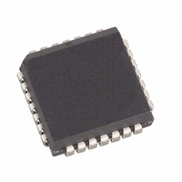
DS2167/DS2168Q ADPCM PROCESSOR 28-PIN PLCC CH1 e1 E2 INCHES DIM. MIN. MAX. A 0.165 0.180 A1 0.090 0.120 A2 0.020 – B 0.026 0.033 B1 0.013 0.021 C 0.009 0.012 D 0.485 0.495 D1 ...