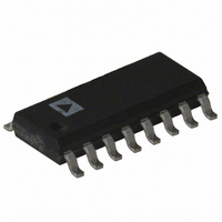
CMP401GSZ Analog Devices Inc, CMP401GSZ Datasheet - Page 2

CMP401GSZ
Manufacturer Part Number
CMP401GSZ
Description
IC COMPARATOR LV 23NS 16-SOIC
Manufacturer
Analog Devices Inc
Type
General Purposer
Datasheet
1.CMP401GRUZ-REEL.pdf
(8 pages)
Specifications of CMP401GSZ
Number Of Elements
4
Output Type
CMOS, TTL
Voltage - Supply
2.7 V ~ 12 V, ±1.35 V ~ 6 V
Mounting Type
Surface Mount
Package / Case
16-SOIC (0.154", 3.90mm Width)
Number Of Elements
4
Technology
BiCMOS
Input Offset Voltage
3@5VmV
Input Bias Current (typ)
3uA
Response Time
33ns
Supply Current (max)
6.5@5V/2mA
Common Mode Rejection Ratio
60dB
Voltage Gain In Db
80dB
Power Supply Rejection Ratio
60dB
Power Supply Requirement
Single/Triple
Single Supply Voltage (max)
16V
Dual Supply Voltage (max)
±8/7V
Operating Temp Range
-40C to 125C
Operating Temperature Classification
Automotive
Mounting
Surface Mount
Pin Count
16
Package Type
SOIC N
Comparator Type
General Purpose
No. Of Comparators
4
Ic Output Type
CMOS, Open-Collector / Drain, TTL
Supply Current
6.5mA
Supply Voltage Range
2.7V To 6V
Rohs Compliant
Yes
Lead Free Status / RoHS Status
Lead free / RoHS Compliant
Available stocks
Company
Part Number
Manufacturer
Quantity
Price
Part Number:
CMP401GSZ
Manufacturer:
ADI/亚德诺
Quantity:
20 000
Part Number:
CMP401GSZ-REEL
Manufacturer:
ADI/亚德诺
Quantity:
20 000
CMP401/CMP402–SPECIFICATIONS
ELECTRICAL SPECIFICATIONS
Parameter
INPUT CHARACTERISTICS
OUTPUT CHARACTERISTICS
POWER SUPPLY
DYNAMIC PERFORMANCE
ELECTRICAL SPECIFICATIONS
Parameter
INPUT CHARACTERISTICS
OUTPUT CHARACTERISTICS
POWER SUPPLY
DYNAMIC PERFORMANCE
Offset Voltage
Hysteresis
Input Bias Current
Input Offset Current
Input Common-Mode Voltage Range
Common-Mode Rejection
Large-Signal Voltage Gain
Offset Voltage Drift
Output High Voltage
Output Low Voltage
Power Supply Rejection Ratio
Analog Supply Current – CMP401
Digital Supply Current – CMP401
Analog Supply Current – CMP401
Digital Supply Current – CMP401
Analog Supply Current – CMP402
Digital Supply Current – CMP402
Analog Supply Current – CMP402
Digital Supply Current – CMP402
Propagation Delay – CMP401
Propagation Delay – CMP402
Offset Voltage
Input Common-Mode Voltage Range
Input Differential Voltage Range
Common-Mode Rejection
Output High Voltage
Output Low Voltage
Power Supply Rejection Ratio
Analog Supply Current – CMP401
Digital Supply Current – CMP401
Analog Supply Current – CMP402
Digital Supply Current – CMP402
Propagation Delay – CMP401
Propagation Delay – CMP402
1
1
V
V
I
I
I
V
CMRR
A
∆V
V
V
PSRR
I
I
I
I
I
I
I
I
t
t
t
t
t
t
V
V
V
CMRR
V
V
PSRR
I
I
I
I
t
t
Symbol
Symbol
P
P
P
P
P
P
P
P
B
B
OS
ANA
DIG
ANA
DIG
ANA
DIG
ANA
DIG
ANA
DIG
ANA
DIG
OS
OS
CM
VO
OH
OL
OS
CM
DIFF
OH
OL
OS
(@ V+
(@ V
/∆T
ANA
ANA
= V
= V+
V+
V+
Conditions
T
T
0.1 V ≤ V
R
I
I
T
V
V
T
V
V
100 mV Step with 20 mV OD
T
100 mV Step with 5 mV OD
T
100 mV Step with 20 mV OD
100 mV Step with 20 mV OD
T
100 mV Step with 5 mV OD
T
100 mV Step with 20 mV OD
Conditions
0.1 V ≤ V
I
I
V
V
100 mV Step with 20 mV OD
100 mV Step with 20 mV OD
DIG
OH
OL
OH
OL
O
O
O
O
O
O
A
A
L
A
A
A
A
A
A
ANA
ANA
= 10 kΩ
DIG
= 25°C
= 25°C
= 25°C
= 0 V, R
= 0 V, R
= 25°C
= 0 V, R
= 0 V, R
= 25°C
= 25°C
= 25°C
= 25°C
= 3.0 V, V
= 0 V, R
= 0 V, R
= 3.2 mA
= 3.2 mA
= –3.2 mA
= –3.2 mA
= 5.0 V, V
and V+
and V+
CM
CM
L
L
L
L
L
L
≤ 3.9 V
CM
≤ 1.9 V
= ∞, T
= ∞
= ∞, T
= ∞
= ∞
= ∞
DIG
DIG
= 0.1 V, T
CM
2.7 V to 6 V
2.7 V to 6 V
= 0.1 V, –40 C ≤ T
A
A
= 25°C
= 25°C
A
= 25 C, unless otherwise noted.)
A
≤ +125 C, unless otherwise noted.)
Min
0
60
4.6
60
Min
0
± 2.0
60
2.6
60
Typ
2
10
1
17
33
54
60
Typ
32
70
Max
4.5
2.0
0.25
6
1
1.2
1
Max
3
4
3
4
± 3
4.0
0.2
6.5
2.0
8.0
2.25
1.4
2.0
1.75
2.25
23
30
65
75
Unit
mV
mV
mV
µA
µA
µA
V
dB
V/mV
µV/°C
V
V
dB
mA
mA
mA
mA
mA
mA
mA
mA
ns
ns
ns
ns
ns
ns
Unit
mV
V
V
dB
V
V
dB
mA
mA
mA
mA
ns
ns


