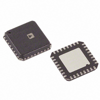
ADCMP567BCPZ Analog Devices Inc, ADCMP567BCPZ Datasheet

ADCMP567BCPZ
Specifications of ADCMP567BCPZ
Available stocks
Related parts for ADCMP567BCPZ
ADCMP567BCPZ Summary of contents
Page 1
FEATURES 250 ps propagation delay input to output 50 ps propagation delay dispersion Differential PECL compatible outputs Differential latch control Robust input protection Input common-mode range −2 +3.0 V Input differential range ±5 V ESD protection >3 kV ...
Page 2
ADCMP567 TABLE OF CONTENTS Specifications..................................................................................... 3 Absolute Maximum Ratings............................................................ 5 Thermal Considerations.............................................................. 5 ESD Caution.................................................................................. 5 Pin Configuration and Function Descriptions............................. 6 Timing Information ......................................................................... 8 Application Information.................................................................. 9 Clock Timing Recovery ............................................................... 9 REVISION HISTORY Revision 0: Initial Version ...
Page 3
SPECIFICATIONS Table 1. ADCMP567 ELECTRICAL CHARACTERISTICS (V Parameter DC INPUT CHARACTERISTICS (See Note) Input Common-Mode Range Input Differential Voltage Input Offset Voltage Input Offset Voltage Channel Matching Offset Voltage Tempco Input Bias Current Input Bias Current Tempco Input Offset Current ...
Page 4
ADCMP567 Parameter AC PERFORMANCE (continued) Equivalent Input Rise Time Bandwidth Toggle Rate Minimum Pulsewidth Unit to Unit Propagation Delay Skew POWER SUPPLY Positive Supply Current Negative Supply Current Logic Supply Current Logic Supply Current Positive Supply Voltage Negative Supply Voltage ...
Page 5
ABSOLUTE MAXIMUM RATINGS Table 2. ADCMP567 Absolute Maximum Ratings Parameter Supply Positive Supply Voltage (V to GND) Voltages CC Negative Supply Voltage (V to GND) EE Logic Supply Voltage (V to GND) DD Ground Voltage Differential Input Input Common-Mode Voltages ...
Page 6
ADCMP567 PIN CONFIGURATION AND FUNCTION DESCRIPTIONS Table 3. ADCMP567 Pin Descriptions Pin No. Mnemonic Function 1 GND Analog Ground 2 −INA Inverting analog input of the differential input stage for Channel A. The inverting A input must be driven in ...
Page 7
Pin No. Mnemonic Function 22 V Negative Supply Terminal Connect. Leave pin unconnected Negative Supply Terminal Logic Supply Terminal One of two complementary outputs for Channel A. QA ...
Page 8
ADCMP567 TIMING INFORMATION LATCH ENABLE LATCH ENABLE DIFFERENTIAL INPUT VOLTAGE Q OUTPUT Q OUTPUT The timing diagram in Figure 3 shows the ADCMP567 compare and latch features. Table 4 describes the terms in the diagram. Table 4. Timing Descriptions Symbol ...
Page 9
APPLICATION INFORMATION The ADCMP567 comparators are very high speed devices. Consequently, high speed design techniques must be employed to achieve the best performance. The most critical aspect of any ADCMP567 design is the use of a low impedance ground plane. ...
Page 10
ADCMP567 as the variation in propagation delay as the input overdrive conditions are changed (Figure 4). For the ADCMP567, overdrive dispersion is typically the overdrive is changed from 100 This specification applies for ...
Page 11
TYPICAL APPLICATION CIRCUITS V IN ADCMP567 V REF LATCH V DD ENABLE INPUTS ALL RESISTORS 50Ω Figure 7. High Speed Sampling Circuits +V REF ADCMP567 V IN ADCMP567 –V REF LATCH V DD ENABLE INPUTS ALL RESISTORS 50Ω Figure 8. ...
Page 12
ADCMP567 TYPICAL PERFORMANCE CHARACTERISTICS ( −5 +3 –2.5 –1.5 –0.5 0.5 NONINVERTING INPUT VOLTAGE (INVERTING VOLTAGE = 0.5V) Figure 12. ...
Page 13
TEMPERATURE (°C) Figure 18. Propagation Delay vs. Temperature 0.2 0.4 0.6 0.8 1.0 ...
Page 14
ADCMP567 OUTLINE DIMENSIONS PIN 1 INDICATOR 12° MAX 1.00 0.90 0.80 ORDERING GUIDE Model Temperature Range ADCMP567BCP −40°C to +85°C 5.00 BSC SQ 0.60 MAX 4.75 BSC SQ 0.50 0.40 0.30 0.80 MAX 0.65 NOM 0.05 MAX 0.02 NOM 0.30 ...
Page 15
Notes Rev Page ADCMP567 ...
Page 16
ADCMP567 Notes © 2003 Analog Devices, Inc. All rights reserved. Trademarks and registered trademarks are the property of their respective owners. C03632–0–10/03(0) Rev Page ...
Page 17
Filename: ADCMP567_Oct 21.doc Directory: C:\Documents and Settings\fburns\Desktop Template: C:\Documents and Settings\aakers\Desktop\Data Sheet Template v3.2.dot Title: ADCMP567 Dual Ultrafast Voltage Comparator Data Sheet (REV. 0) Subject: Author: Analog Devices, Inc. Keywords: Comments: Creation Date: 10/15/2003 1:35 PM Change Number: 15 Last ...


