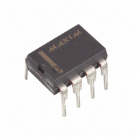
MAX931CPA+ Maxim Integrated Products, MAX931CPA+ Datasheet - Page 9

MAX931CPA+
Manufacturer Part Number
MAX931CPA+
Description
IC COMPARATOR SNGL W/REF LP 8DIP
Manufacturer
Maxim Integrated Products
Type
with Voltage Referencer
Datasheet
1.MAX931CSA.pdf
(16 pages)
Specifications of MAX931CPA+
Number Of Elements
1
Output Type
CMOS, TTL
Voltage - Supply
2.5 V ~ 11 V, ±1.25 V ~ 5.5 V
Mounting Type
Through Hole
Package / Case
8-DIP (0.300", 7.62mm)
Number Of Channels
1 Channel
Supply Voltage (max)
11 V
Supply Voltage (min)
2.5 V
Supply Current (max)
3.2 uA
Maximum Operating Temperature
+ 70 C
Mounting Style
Through Hole
Minimum Operating Temperature
0 C
Propagation Delay Time
12 us
Comparator Type
General Purpose
No. Of Comparators
1
Response Time
12µs
Ic Output Type
CMOS, TTL
Supply Current
2.5µA
Supply Voltage Range
± 1.25V To ± 5.5V
Amplifier Case Style
DIP
Rohs Compliant
Yes
Output Compatibility
CMOS, TTL
Lead Free Status / RoHS Status
Lead free / RoHS Compliant
current falls. The reference will not function below
about 2.2V, although the comparators will continue to
operate with a total supply voltage as low as 1V. While
the MAX934 has comparators that may be used at
supply voltages below 2V, the MAX931, MAX932, and
MAX933 may not be used with supply voltages
significantly below 2.5V.
At low supply voltages, the comparators’ output drive is
reduced and the propagation delay increases (see
Typical Operating Characteristics ). The useful input
voltage range extends from the negative supply to a
little under 1V below the positive supply, which is
slightly closer to the positive rail than the device
operating from higher supply voltages. Test your
prototype over the full temperature and supply-voltage
range if operation below 2.5V is anticipated.
With 100mV of overdrive, propagation delay is typically
3µs. The Typical Operating Characteristics show the
propagation delay for various overdrive levels.
The MAX931 and MAX934 output swings from V+ to
GND, so TTL compatibility is assured by using a
+5V ±10% supply. The negative supply does not affect
the output swing, and can range from 0V to -5V ±10%.
The MAX932 and MAX933 do not have a GND pin, and
their outputs swing from V+ to V-. Connect V- to ground
and V+ to a +5V supply to achieve TTL compatibility.
The MAX931-MAX934’s unique design achieves an
output source current of more than 40mA and a
sink current of over 5mA, while keeping quiescent
currents in the microampere range. The output can
source 100mA (at V+ = 5V) for short pulses, as long as
the package's maximum power dissipation is not
exceeded. The output stage does not generate crowbar
switching currents during transitions, which minimizes
feedback through the supplies and helps ensure stability
without bypassing.
The internal bandgap voltage reference has an output
of 1.182V above V-. Note that the REF voltage is
referenced to V-, not to GND. Its accuracy is ±2% in
the range 0°C to +70°C. The REF output is typically
capable of sourcing 15µA and sinking 8µA. Do not
bypass the REF output. For applications that require a
1% precision reference, see the MAX921-MAX924
data sheet.
Although the comparators have a very high gain, useful
gain is limited by noise. This is shown in the Transfer
Function graph (see Typical Operating Characteristics ).
_______________________________________________________________________________________
Noise Considerations
Comparator Output
Voltage Reference
Comparators with 2% Reference
Ultra Low-Power, Low-Cost
As the input voltage approaches the comparator's
offset, the output begins to bounce back and forth; this
peaks when V
the graph averages out the bouncing, making the
transfer function easy to observe.) Consequently, the
comparator has an effective wideband peak-to-peak
noise of around 0.3mV. The voltage reference has
peak-to peak noise approaching 1mV. Thus, when a
comparator is used with the reference, the combined
peak-to-peak noise is about 1mV. This, of course, is
much higher than the RMS noise of the individual
components. Care should be taken in the layout to
avoid capacitive coupling from any output to the
reference pin. Crosstalk can significantly increase the
actual noise of the reference.
Hysteresis increases the comparators’ noise margin by
increasing the upper threshold and decreasing the
lower threshold (see Figure 2).
To add hysteresis to the MAX931/MAX932/MAX933,
connect resistor R1 between REF and HYST, and
connect resistor R2 between HYST and V- (Figure 3). If
no hysteresis is required, connect HYST to REF. When
hysteresis is added, the upper threshold increases by
the same amount that the lower threshold decreases.
The hysteresis band (the difference between the upper
and lower thresholds, V
twice the voltage between REF and HYST. The HYST
input can be adjusted to a maximum voltage of REF
and to a minimum voltage of (REF - 50mV). The
Figure 2. Threshold Hysteresis Band
__________Applications Information
VREF - VHYST
OUT
IN+
IN-
Hysteresis (MAX931/MAX932/MAX933)
IN
V
HB
= V
OS
. (The lowpass filter shown on
HB
THRESHOLDS
HYSTERESIS
) is approximately equal to
BAND
Hysteresis
9


