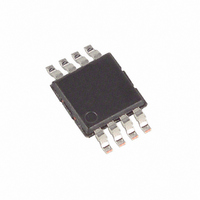
MAX933CUA+ Maxim Integrated Products, MAX933CUA+ Datasheet - Page 2

MAX933CUA+
Manufacturer Part Number
MAX933CUA+
Description
IC COMPARATOR W/REF 8-UMAX
Manufacturer
Maxim Integrated Products
Type
with Voltage Referencer
Datasheet
1.MAX931CSA.pdf
(16 pages)
Specifications of MAX933CUA+
Number Of Elements
2
Output Type
CMOS, TTL
Voltage - Supply
2.5 V ~ 11 V, ±1.25 V ~ 5.5 V
Mounting Type
Surface Mount
Package / Case
8-TSSOP, 8-MSOP (0.118", 3.00mm Width)
Number Of Channels
2 Channels
Supply Voltage (max)
5.5 V
Supply Voltage (min)
1.25 V
Supply Current (max)
4.5 uA
Maximum Operating Temperature
+ 70 C
Mounting Style
SMD/SMT
Minimum Operating Temperature
0 C
Propagation Delay Time
12 us
Lead Free Status / RoHS Status
Lead free / RoHS Compliant
ELECTRICAL CHARACTERISTICS—5V Operation
(V+ = 5V, V- = GND = 0V, T
ABSOLUTE MAXIMUM RATINGS
V+ to V-, V+ to GND, GND to V-................................-0.3V, +12V
Inputs
Outputs
Ultra Low-Power, Low-Cost
Comparators with 2% Reference
Stresses beyond those listed under “Absolute Maximum Ratings” may cause permanent damage to the device. These are stress ratings only, and functional
operation of the device at these or any other conditions beyond those indicated in the operational sections of the specifications is not implied. Exposure to
absolute maximum rating conditions for extended periods may affect device reliability.
2
Supply Voltage Range
Supply Current
Input Offset Voltage
Input Leakage Current (IN-, IN+)
Input Leakage Current (HYST)
Input Common-Mode Voltage Range
Common-Mode Rejection Ratio
Power-Supply Rejection Ratio
Voltage Noise
Hysteresis Input Voltage Range
Response Time
POWER REQUIREMENTS
COMPARATOR
Current, IN_+, IN_-, HYST...............................................20mA
Voltage, IN_+, IN_-, HYST................(V+ + 0.3V) to (V- – 0.3V)
Current, REF....................................................................20mA
Current, OUT_ .................................................................50mA
Voltage, REF ....................................(V+ + 0.3V) to (V- – 0.3V)
Voltage, OUT_ (MAX931/934) .....(V+ + 0.3V) to (GND – 0.3V)
Voltage, OUT_ (MAX932/933)..........(V+ + 0.3V) to (V- – 0.3V)
OUT_ Short-Circuit Duration (V+ ≤ 5.5V) ...............Continuous
_______________________________________________________________________________________
PARAMETER
A
= T
MIN
to T
MAX
IN+ = IN- + 100mV
(Note 1)
V
IN+ = IN- = 2.5V, C/E temp. ranges
MAX931, MAX932, MAX933
V- to (V+ – 1.3V)
V+ = 2.5V to 11V
100Hz to 100kHz
MAX931, MAX932, MAX933
T
A
CM
, unless otherwise noted.)
= +25°C, 100pF load
= 2.5V
CONDITIONS
MAX931,
HYST = REF
MAX932,
HYST = REF
MAX933,
HYST = REF
MAX934
Continuous Power Dissipation (T
Operating Temperature Ranges:
Storage Temperature Range .............................-65°C to +150°C
Lead Temperature (soldering, 10sec) .............................+300°C
16-Pin Plastic DIP (derate 10.53mW/°C above +70°C)..842mW
16-Pin SO (derate 8.70mW/°C above +70°C) ................696mW
8-Pin Plastic DIP (derate 9.09mW/°C above +70°C) ...727mW
8-Pin SO (derate 5.88mW/°C above +70°C)................471mW
8-Pin µMAX (derate 4.1mW/°C above +70°C) .............330mW
MAX93_C_ _ .......................................................0°C to +70°C
MAX93_E_ _.....................................................-40°C to +85°C
T
C/E temp. ranges
T
C/E temp. ranges
T
C/E temp. ranges
T
C/E temp. ranges
Overdrive = 10mV
Overdrive = 100mV
A
A
A
A
= +25°C
= +25°C
= +25°C
= +25°C
REF – 0.05
MIN
2.5
V-
A
= +70°C)
±0.01
±0.02
TYP
2.5
3.1
3.1
5.5
0.1
0.1
20
12
4
V+ – 1.3
MAX
±10
REF
3.2
4.5
4.5
6.5
8.5
1.0
1.0
±5
11
4
6
6
UNITS
µV
mV/V
mV/V
mV
µA
nA
nA
µs
V
V
RMS
V


