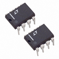
LT1016CN8 Linear Technology, LT1016CN8 Datasheet - Page 6

LT1016CN8
Manufacturer Part Number
LT1016CN8
Description
IC COMPARATOR 10NS HI-SPEED 8DIP
Manufacturer
Linear Technology
Series
UltraFast™r
Type
General Purposer
Datasheet
1.LT1016CN8PBF.pdf
(20 pages)
Specifications of LT1016CN8
Number Of Elements
1
Output Type
CMOS, Complementary, TTL
Mounting Type
Through Hole
Package / Case
8-DIP (0.300", 7.62mm)
Lead Free Status / RoHS Status
Contains lead / RoHS non-compliant
Available stocks
Company
Part Number
Manufacturer
Quantity
Price
Company:
Part Number:
LT1016CN8
Manufacturer:
LT
Quantity:
10 300
Part Number:
LT1016CN8
Manufacturer:
LINEAR/凌特
Quantity:
20 000
Part Number:
LT1016CN8#PBF
Manufacturer:
LINEAR/凌特
Quantity:
20 000
APPLICATIO S I FOR ATIO
LT1016
Common Mode Considerations
The LT1016 is specified for a common mode range of
–3.75V to 3.5V with supply voltages of ±5V. A more
general consideration is that the common mode range is
1.25V above the negative supply and 1.5V below the
positive supply, independent of the actual supply voltage.
The criteria for common mode limit is that the output still
responds correctly to a small differential input signal.
Either input may be outside the common mode limit (up to
the supply voltage) as long as the remaining input is within
the specified limit, and the output will still respond cor-
rectly. There is one consideration, however, for inputs that
exceed the positive common mode limit. Propagation
delay will be increased by up to 10ns if the signal input is
more positive than the upper common mode limit and then
switches back to within the common mode range. This
effect is not seen for signals more negative than the lower
common mode limit.
Input Impedance and Bias Current
Input bias current is measured with the output held at
1.4V. As with any simple NPN differential input stage, the
LT1016 bias current will go to zero on an input that is low
and double on an input that is high. If both inputs are less
than 0.8V above V
zero. If either input exceeds the positive common mode
limit, input bias current will increase rapidly, approaching
several milliamperes at V
Differential input resistance at zero differential input
voltage is about 10kW, rapidly increasing as larger DC
differential input signals are applied. Common mode input
resistance is about 4MW with zero differential input
voltage. With large differential input signals, the high input
will have an input resistance of about 2MW and the low
input greater than 20MW.
6
–
U
, both input bias currents will go to
IN
U
= V
+
.
W
U
Input capacitance is typically 3.5pF. This is measured by
inserting a 1k resistor in series with the input and measur-
ing the resultant change in propagation delay.
LATCH Pin Dynamics
The LATCH pin is intended to retain input data (output
latched) when the LATCH pin goes high. This pin will float
to a high state when disconnected, so a flowthrough
condition requires that the LATCH pin be grounded. To
guarantee data retention, the input signal must be valid at
least 5ns before the latch goes high (setup time) and must
remain valid at least 3ns after the latch goes high (hold
time). When the latch goes low, new data will appear at the
output in approximately 8ns to 10ns. The LATCH pin is
designed to be driven with TTL or CMOS gates. It has no
built-in hysteresis.
Measuring Response Time
The LT1016 is able to respond quickly to fast low level
signals because it has a very high gain-bandwidth product
(ª50GHz), even at very high frequencies. To properly
measure the response of the LT1016 requires an input
signal source with very fast rise times and exceptionally
clean settling characteristics. This last requirement comes
about because the standard comparator test calls for an
input step size that is large compared to the overdrive
amplitude. Typical test conditions are 100mV step size
with only 5mV overdrive. This requires an input signal that
settles to within 1% (1mV) of final value in only a few
nanoseconds with no ringing or “long tailing.” Ordinary
high speed pulse generators are not capable of generating
such a signal, and in any case, no ordinary oscilloscope is
capable of displaying the waveform to check its fidelity.
Some means must be used to inherently generate a fast,
clean edge with known final value.


