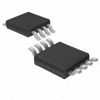
LT1720IMS8#TRPBF Linear Technology, LT1720IMS8#TRPBF Datasheet - Page 8

LT1720IMS8#TRPBF
Manufacturer Part Number
LT1720IMS8#TRPBF
Description
IC COMPARATOR DUAL HS 3/5V 8MSOP
Manufacturer
Linear Technology
Series
UltraFast™r
Type
General Purposer
Datasheet
1.LT1720CS8PBF.pdf
(28 pages)
Specifications of LT1720IMS8#TRPBF
Number Of Elements
2
Output Type
CMOS, Rail-to-Rail, TTL
Voltage - Supply
2.7 V ~ 6 V
Mounting Type
Surface Mount
Package / Case
8-TSSOP, 8-MSOP (0.118", 3.00mm Width)
Lead Free Status / RoHS Status
Lead free / RoHS Compliant
Available stocks
Company
Part Number
Manufacturer
Quantity
Price
LT1720/LT1721
APPLICATIONS INFORMATION
Input Voltage Considerations
The LT1720/LT1721 are specifi ed for a common mode range
of –100mV to 3.8V when used with a single 5V supply. In
general the common mode range is 100mV below ground
to 1.2V below V
limit is that the output still responds correctly to a small
differential input signal. Also, if one input is within the
common mode limit, the other input signal can go outside
the common mode limits, up to the absolute maximum
limits (a diode drop past either rail at 10mA input current)
and the output will retain the correct polarity.
When either input signal falls below the negative common
mode limit, the internal PN diode formed with the substrate
can turn on, resulting in signifi cant current fl ow through
the die. An external Schottky clamp diode between the
input and the negative rail can speed up recovery from
negative overdrive by preventing the substrate diode from
turning on.
When both input signals are below the negative common
mode limit, phase reversal protection circuitry prevents
false output inversion to at least –400mV common mode.
However, the offset and hysteresis in this mode will increase
dramatically, to as much as 15mV each. The input bias
currents will also increase.
When both input signals are above the positive common
mode limit, the input stage will become debiased and
the output polarity will be random. However, the internal
hysteresis will hold the output to a valid logic level, and
because the biasing of each comparator is completely
independent, there will be no impact on any other com-
parator. When at least one of the inputs returns to within
the common mode limits, recovery from this state will
take as long as 1μs.
The propagation delay does not increase signifi cantly when
driven with large differential voltages. However, with low
levels of overdrive, an apparent increase may be seen with
large source resistances due to an RC delay caused by the
2pF typical input capacitance.
8
CC
. The criterion for this common mode
Input Protection
The input stage is protected against damage from large
differential signals, up to and beyond a differential voltage
equal to the supply voltage, limited only by the absolute
maximum currents noted. External input protection cir-
cuitry is only needed if currents would otherwise exceed
these absolute maximums. The internal catch diodes can
conduct current up to these rated maximums without
latchup, even when the supply voltage is at the absolute
maximum rating.
The LT1720/LT1721 input stage has general purpose
internal ESD protection for the human body model. For
use as a line receiver, additional external protection may
be required. As with most integrated circuits, the level
of immunity to ESD is much greater when residing on a
printed circuit board where the power supply decoupling
capacitance will limit the voltage rise caused by an ESD
pulse.
Unused Inputs
The inputs of any unused compartor should be tied off in
a way that defi nes the output logic state. The easiest way
to do this is to tie IN
Input Bias Current
Input bias current is measured with both inputs held at 1V.
As with any PNP differential input stage, the LT1720/LT1721
bias current fl ows out of the device. With a differential
input voltage of even just 100mV or so, there will be zero
bias current into the higher of the two inputs, while the
current fl owing out of the lower input will be twice the
measured bias current. With more than two diode drops
of differential input voltage, the LT1720/LT1721’s input
protection circuitry activates, and current out of the lower
input will increase an additional 30% and there will be a
small bias current into the higher of the two input pins,
of 4μA or less. See the Typical Performance curve “Input
Current vs Differential Input Voltage.”
+
to V
CC
and IN
–
to GND.
17201fc


