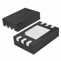
LT6700MPDCB-3#TRPBF Linear Technology, LT6700MPDCB-3#TRPBF Datasheet - Page 16

LT6700MPDCB-3#TRPBF
Manufacturer Part Number
LT6700MPDCB-3#TRPBF
Description
IC COMP DUAL 400MV REF 6-DFN
Manufacturer
Linear Technology
Series
Over-The-Top®r
Type
General Purposer
Datasheet
1.LT6700CS6-3TRMPBF.pdf
(20 pages)
Specifications of LT6700MPDCB-3#TRPBF
Number Of Elements
2
Output Type
Open Collector
Voltage - Supply
1.4 V ~ 18 V
Mounting Type
Surface Mount
Package / Case
6-WFDFN Exposed Pad
Lead Free Status / RoHS Status
Lead free / RoHS Compliant
Available stocks
Company
Part Number
Manufacturer
Quantity
Price
applicaTions inForMaTion
LT6700/LT6700HV
charges and discharges in a shallow, controlled fashion.
The multiplied reference signal also contains ripple that is
the hysteresis multiplied by the same factor, so additional
filtering is performed at the sense node of the bridge to
prevent comparator chatter in the section A comparator,
which is performing the actual conditional decision for
the circuit.
Instrumentation Grade Pulse Width Modulator (PWM)
Comparators with hysteresis are frequently employed
to make simple oscillator structures, and the LT6700/
3.3µF
Figure 2. Micropower Thermostat/Temperature Alarm
R
R
*RESISTANCE MAY REQUIRE OPTIMIZATION FOR OPERATION
HYSTERESIS ZONE ≈0.4°C
OVER INTENDED R
TH
SET
R
= 1M (e.g., YSI 44015, 1.00MΩ AT 25°C)
TH
= R
2 • V
TH
AT T
REF
R
T
SET
0V TO 2V
SET
V
22µF
+
–
IN
TH
499k
499k
AND V
**
††
*
†
10k**
1% METAL FILM
DELETE FOR PWM MODE
CONNECT FOR PWM MODE
OPTIMIZED FOR 2kHz ΔΣ SAMPLING, f
0.1µF
SUPPLY
+INA
–INB OUTB
LT6700-1
NC7S14
GND
V
309k*
5 • V
S
OUTA
RANGES
REF
= 2V
0.22µF
10k
309k*
6700123 F02
220k
††
Figure 3. Isolated PWM or ∆∑ Converter
470Ω
100k*
220k*
COIN CELL
T < T
3.3µF
1.4V TO 18V
(I
S
Lithium
≈ 10µA)
SET
412k*
100k*
PWM(MAX)
3V NOM (I
+
+INA
–INB OUTB
LT6700-1
≈ 0.6kHz
GND
V
S
OUTA
S
< 3mA)
LT6700HV lends itself nicely to forming a charge-balancing
PWM function. The circuit shown in Figure 3 forms a PWM
that is intended to transmit an isolated representation of a
voltage difference, rather like an isolated instrumentation
amplifier. The section B comparator is used to generate a
2V reference supply level for the CMOS NOT gate (inverter),
which serves as the precision switch element for the charge
balancer. The heart of the charge balancer is the section A
comparator, which is detecting slight charge or discharge
states on the 0.22µF “integration” capacitor as it remains
balanced at ≈400mV by feedback through the NOT gate.
The input sense voltage, V
ance current that the NOT gate duty cycle is continually
correcting for, thus the digital waveform at the section A
comparator output is a PWM representation of V
respect to the 2V “full scale.” In this particular circuit, the
PWM information drives the LED of an opto-coupler, allow-
ing the V
barrier. As an additional option to the circuit, the feedback
loop can be broken and a second opto-coupler employed to
provide the charge balance management. This configura-
tion allows for clocking the comparator output (externally
to this circuit) and providing synchronous feedback such
that a simple Δ∑ voltage-to-frequency conversion can be
formed if desired. Approximately 11-bit accuracy and noise
performance was observed in a one second integration
period for duty factors from 1% to 99%.
0.1µF
10k
0.1µF
10k
IN
6700123 F03
information to be coupled across a dielectric
10k
750Ω
†
6
5
1
2
SAMPLE
3V/5V
3V/5V
ΔΣ
IN
6
5
1
2
10k
750**
MOC-207
IN
MOC-207**
PWM OUT
(OR ΔΣ SENSE)
, is converted to an imbal-
IN
6700123fg
with


