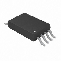
AD8561ARU-REEL Analog Devices Inc, AD8561ARU-REEL Datasheet

AD8561ARU-REEL
Specifications of AD8561ARU-REEL
Available stocks
Related parts for AD8561ARU-REEL
AD8561ARU-REEL Summary of contents
Page 1
FEATURES 7 ns Propagation Delay Single Supply Operation Low Power Latch Function TSSOP Packages APPLICATIONS High Speed Timing Clock Recovery and Clock Distribution Line Receivers Digital Communications Phase Detectors High Speed ...
Page 2
AD8561–SPECIFICATIONS ELECTRICAL SPECIFICATIONS Parameter INPUT CHARACTERISTICS Offset Voltage Offset Voltage Drift Input Bias Current Input Offset Current Input Common-Mode Voltage Range Common-Mode Rejection Ratio Large Signal Voltage Gain Input Capacitance LATCH ENABLE INPUT Logic “1” Voltage Threshold Logic “0” Voltage ...
Page 3
ELECTRICAL SPECIFICATIONS Parameter INPUT CHARACTERISTICS Offset Voltage Offset Voltage Drift Input Bias Current Input Offset Current Input Common-Mode Voltage Range Common-Mode Rejection Ratio Large Signal Voltage Gain Input Capacitance LATCH ENABLE INPUT Logic “1” Voltage Threshold Logic “0” Voltage Threshold ...
Page 4
... Lead Temperature Range (Soldering, 10 sec +300 C Temperature Model Range AD8561AN – +85 C AD8561ARU – +85 C AD8561AR – +85 C CAUTION ESD (electrostatic discharge) sensitive device. Electrostatic charges as high as 4000 V readily accumulate on the human body and test equipment and can discharge without detection. ...
Page 5
Typical Performance Characteristics 5 +125 5V, SINGLE SUPPLY S 4 – + –2.5 –2.0 –1.5 –1.0 –0.5 0 0.5 1.0 1.5 DIFFERENTIAL INPUT VOLTAGE – mV Figure 1. Output Voltage vs. ...
Page 6
AD8561 0.5 0.4 0 – +125 SINK CURRENT – mA Figure 10. Output Low Voltage vs. ...
Page 7
APPLICATIONS OPTIMIZING HIGH SPEED PERFORMANCE As with any high speed comparator or amplifier, proper design and layout techniques should be used to ensure optimal perfor- mance from the AD8561. The performance limits of high speed circuitry can easily be a ...
Page 8
AD8561 INPUT STAGE AND BIAS CURRENTS The AD8561 uses a PNP differential input stage that enables the input common-mode range to extend all the way from the negative supply rail to within 2 the positive supply rail. The ...
Page 9
SPICE Model * AD8561 SPICE Macro-Model Typical Values * 4/98, Ver. 1.0 * TAM / ADSC * * Node assignments * non-inverting input * | inverting input * | | * | | * | | * | | * ...
Page 10
AD8561 GSY1 99 52 POLY(1) (99,50) 4E-3 -2.6E-4 GSY2 52 50 POLY(1) (99,50) 3.7E-3 -.6E-3 RSY Gain Stage Av=250 fp=100MHz * (12,98) 0. 1000 10E-13 D2 ...
Page 11
REV. 0 OUTLINE DIMENSIONS Dimensions shown in inches and (mm). 8-Lead Plastic DIP (N-8) 0.430 (10.92) 0.348 (8.84 0.280 (7.11) 0.240 (6.10 0.325 (8.25) 0.300 (7.62) 0.060 (1.52) PIN 1 ...


