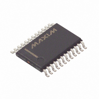
MAX9602EUG+ Maxim Integrated Products, MAX9602EUG+ Datasheet - Page 11

MAX9602EUG+
Manufacturer Part Number
MAX9602EUG+
Description
IC COMPARATOR HS 24-TSSOP
Manufacturer
Maxim Integrated Products
Type
General Purposer
Datasheet
1.MAX9600EUP.pdf
(12 pages)
Specifications of MAX9602EUG+
Number Of Elements
4
Output Type
Complementary, Differential, PECL
Mounting Type
Surface Mount
Package / Case
24-TSSOP
Number Of Channels
4 Channels
Product
Digital Comparators
Offset Voltage (max)
+/- 9 mV
Input Bias Current (max)
20 uA
Supply Voltage (max)
5 V
Supply Voltage (min)
1 V
Supply Current (max)
10000 uA
Maximum Power Dissipation
975 mW
Maximum Operating Temperature
+ 85 C
Mounting Style
SMD/SMT
Minimum Operating Temperature
- 40 C
Comparator Type
High Speed
No. Of Comparators
4
Response Time
500ps
Ic Output Type
Differential, PECL
Supply Current
28mA
Supply Voltage Range
4.3V To 6.3V, -4V To -6V
Rohs Compliant
Yes
Lead Free Status / RoHS Status
Lead free / RoHS Compliant
The timing diagram (Figure 1) illustrates the operation
of a comparator with latch enable. The top line of the
diagram illustrates a latch-enable pulse. Initially, the
latch-enable input (LE, LE_) is differentially high, which
places the comparator in latch mode. When the input
signal (IN_+, IN_-) switches from low to high, the output
(Q_, Q_) remains latched to the previous low state.
When the latch-enable input goes differentially low,
starting the compare function, the output responds to
the input and transitions to high after a time (t
leading edges of the subsequent input signal switch
the comparator after time interval t
ing on the direction of the input transitions) until a high
latch-enable pulse places the device in latch mode
again. The input signal must occur at minimum time
(t
state for at least t
latch-pulse width (t
proper latch operation.
LS
Timing Information (MAX9600/MAX9601)
) before the latch rising edge, and must maintain its
TOP VIEW
HYSA
INA+
GND
INA-
LEA
LEA
V
V
QA
QA
CC
EE
10
1
2
3
4
5
6
7
8
9
LH
______________________________________________________________________________________
LPW
TSSOP-20
after the rising edge. A minimum
MAX9600
) of 250ps (typ) is needed for
Dual ECL and Dual/Quad PECL, 500ps,
20
19
18
17
16
15
14
13
12
11
PD+
QB
QB
GND
LEB
LEB
V
V
HYSB
INB-
INB+
EE
CC
or t
Ultra-High-Speed Comparators
PD-
V
HYSA
CCOA
INA+
INA-
LEA
LEA
V
V
QA
QA
LPD
CC
(depend-
EE
10
1
2
3
4
5
6
7
8
9
). The
TSSOP-20
MAX9601
The MAX9600/MAX9601/MAX9602 outputs are emitter
followers that require external resistive connections to a
voltage source (V
for proper static and dynamic operation. When properly
terminated, the outputs provide appropriate levels, V
or V
MAX9602). Output-current polarity always sinks into the
termination scheme during proper operation.
ECL-output signal levels are referenced to GND, and
PECL-output signals are referenced to V
MAX9600 TRANSISTOR COUNT: 558
MAX9601 TRANSISTOR COUNT: 600
MAX9602 TRANSISTOR COUNT: 608
PROCESS: Bipolar
OH
20
19
18
17
16
15
14
13
12
11
QB
V
LEB
LEB
V
V
HYSB
INB-
INB+
QB
, for ECL (MAX9600) or PECL (MAX9601/
CCOB
EE
CC
INC+
IND+
INA+
INB+
INA-
INB-
INC-
IND-
V
V
V
V
CC
CC
EE
EE
T
) more negative than the lowest V
10
11
12
1
2
3
4
5
6
7
8
9
TSSOP-24
MAX9602
Pin Configurations
Chip Information
24
23
22
21
20
19
18
17
16
15
14
13
V
QA
QA
V
QB
QB
V
QC
QC
V
QD
QD
CCOA
CCOB
CCOC
CCOD
CCO
_.
ECL/PCL
OL
OL
11


