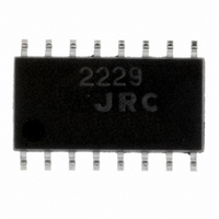
NJM2229M NJR, NJM2229M Datasheet - Page 4

NJM2229M
Manufacturer Part Number
NJM2229M
Description
IC SYNCH SEPARATOR W/AFC 16-DMP
Manufacturer
NJR
Type
Synchronous Separatorr
Datasheet
1.NJM2229M.pdf
(9 pages)
Specifications of NJM2229M
Mounting Type
Surface Mount
Package / Case
16-DMP
Lead Free Status / RoHS Status
Contains lead / RoHS non-compliant
Applications
-
Available stocks
Company
Part Number
Manufacturer
Quantity
Price
Company:
Part Number:
NJM2229M
Manufacturer:
FUJI
Quantity:
225
Part Number:
NJM2229M
Manufacturer:
JRC
Quantity:
20 000
Part Number:
NJM2229M(TE1)
Manufacturer:
JRC
Quantity:
20 000
■ ELECTRICAL PARAMETER TEST METHOD
Operating Current
AFC Free-run Frequency
AFC pulse Width
AFC Output Delay Time
AFC Lock Range
AFC Capture Range
AFC Output Voltage
Sync. Signal Detection level
Sync. Signal Detection Output Voltage
Sync. Signal Detection Delay time
V
V
V
V
V
Sync. Detection Lock Voltage High
Sync. Detection Lock Voltage Low
Sync. Detection Capture High
Sync. Detection Capture Low
Sync. Detection Output Voltage
Sync.
- 4 -
Test circuit
SYNC
SYNC
SYNC
SYNC
SYNC
Threshold Voltage High
Threshold Voltage Low
Output Voltage
Pulse Width
Delay Time
Detection
PARAMETER
Output
Voltage
SW-1
A
A
A
A
A
A
B
B
A
A
A
A
A
A
A
A
A
A
B
A
A
SW-2
A
A
A
A
A
A
A
A
A
A
A
A
A
A
A
B
B
B
B
B
B
SW-3
A
A
A
A
A
A
A
A
A
A
A
A
A
A
A
B
B
B
B
B
B
No input signal. DC current at Pin 15.
No input signal. Video-IN terminal to GND. Frequency at
Pin 16.
No input signal. Output Pulse width at Pin 16. (Note 1)
Input 2Vp-p video signal on Video-IN terminal. Delay
time between input and AFC output signal. (Note 1)
Operating frequency range of AFC output when the input
Pulse signal frequency with 5 µsec pulse width at
Video-IN terminal changes.
Frequency range when signal changes from AFC unlock
condition to look.
Output voltage at Pin 16 in condition of load resistance
R
Putting 2Vp-p video signal on Video-IN terminal and
reducing it to the level that pin5 output waveform is
beginning to change. V
point. (Note 2)
Output voltage at Pin5 with load resistance R
2Vp-p video signal at Video-IN terminal. Time difference
between input(Pin5) and output(Pin6) waveform.
Gradually increase DC voltage from 2V to 3V at V
terminal. DC input voltage when output voltage at Pin10
changes from Low to High state.
Gradually decrease DC voltage from 3V to 1V at
V
at Pin10 changes from High to Low state.
Output voltage at Pin10 with load resistance R
Putting 2Vp-p video signal on Video-IN terminal and
measurring output pulse width at Pin10. (Note 3)
Putting 2Vp-p video signal on Video-IN terminal Delay
time between output at Pin10 and V
3)
Increase DC voltage from 2V to 4V put on Sync-Det-IN
terminal and measure its DC voltage when output
voltage at Pin13 changes from HIGH to Low. (Note 4)
Decrease DC voltage from 2V to 1V put on Sync-Det-IN
terminal and measure its DC voltage when output
voltage at Pin13 changes from HIGH to Low. (Note 4)
Decrease DC voltage from 3V to 1V put on Sync-Det-IN
terminal and measure its DC voltage when output
voltage at Pin13 changes from Low to HIGH. (Note 4)
Increase DC voltage from 1V to 2V put on Sync-Det-IN
terminal and measure its DC voltage when output
voltage at Pin13 changes from Low to HIGH. (Note 4)
Output voltage at Pin13 with load resistance R
Output voltage at Pin14 with load resistance R
SYNC
L
=10kΩ
-IN terminal. DC input voltage when output voltage
TEST CONDITION.
HDS
is the sink-chip level at that
SYNC
at Pin6. (Note
Ver.2004-02-17
L
=10kΩ.
L
L
L
=10kΩ
=10kΩ.
=10kΩ.
SYNC
-IN


