AP730P Advanced Power Electronics Corp., AP730P Datasheet

The Advanced Power MOSFETs from APEC provide the designer with the best combination of fast switching ,ruggedized device design , low on-resistance and cost-effectiveness

AP730P

Manufacturer Part Number
AP730P
Description
The Advanced Power MOSFETs from APEC provide the designer with the best combination of fast switching ,ruggedized device design , low on-resistance and cost-effectiveness
Manufacturer
Advanced Power Electronics Corp.
Datasheet

Specifications of AP730P

Vds
400V
Vgs
±30V
Rds(on) / Max(m?) Vgs@10v
1000
Qg (nc)
35
Qgs (nc)
3.7
Qgd (nc)
20
Id(a)
5.5
Pd(w)
74
Configuration
Single N
Package
TO-220
▼ ▼ ▼ ▼ Dynamic dv/dt Rating
▼ ▼ ▼ ▼ Repetitive Avalanche Rated
▼ ▼ ▼ ▼ Fast Switching
▼ ▼ ▼ ▼ Simple Drive Requirement
V
V
I
I
I
P
E
I
E
T
T
Rthj-c
Rthj-a
Data & specifications subject to change without notice
Description
Absolute Maximum Ratings
Thermal Data
The Advanced Power MOSFETs from APEC provide the
designer with the best combination of fast switching ,
ruggedized device design , low on-resistance and cost-effectiveness.
The TO-220 package is universally preferred for all commercial-industrial
applications. The device is suited for switch mode power supplies ,DC-
AC converters and high current high speed switching circuits.
D
D
DM
AR
STG
J
DS
GS
D
AS
AR
@T
@T
@T
C
C
Symbol
Symbol
C
=25℃
=100℃
=25℃
Advanced Power
Electronics Corp.
Drain-Source Voltage
Gate-Source Voltage
Continuous Drain Current, V
Pulsed Drain Current
Total Power Dissipation
Linear Derating Factor
Single Pulse Avalanche Energy
Avalanche Current
Repetitive Avalanche Energy
Storage Temperature Range
Operating Junction Temperature Range
Thermal Resistance Junction-case
Thermal Resistance Junction-ambient
Parameter
1
Parameter
G
D
GS
GS
S
@ 10V
@ 10V
2
TO-220
N-CHANNEL ENHANCEMENT MODE
POWER MOSFET
Max.
Max.
-55 to 150
-55 to 150
Rating
BV
R
I
± 30
D
0.59
G
400
260
5.5
3.5
5.5
23
74
DS(ON)
7
DSS
Value
1.7
62
AP730P
D
S
1.0Ω
400V
5.5A
Units
W/℃
℃/W
℃/W
200219032
Unit
W
mJ
mJ
V
V
A
A
A
A

Related parts for AP730P

AP730P Summary of contents

Page 1

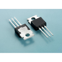
... Thermal Data Symbol Rthj-c Thermal Resistance Junction-case Rthj-a Thermal Resistance Junction-ambient Data & specifications subject to change without notice N-CHANNEL ENHANCEMENT MODE POWER MOSFET G D TO-220 S Parameter @ 10V GS @ 10V Parameter AP730P BV 400V DSS R 1.0Ω DS(ON Rating Units 400 ± 30 5.5 3 0.59 W/℃ ...

Page 2

... AP730P Electrical Characteristics@T Symbol Parameter BV Drain-Source Breakdown Voltage DSS ΔBV Breakdown Voltage Temperature Coefficient /ΔT DSS j R Static Drain-Source On-Resistance DS(ON) V Gate Threshold Voltage GS(th) g Forward Transconductance fs I Drain-Source Leakage Current (T DSS Drain-Source Leakage Current (T I Gate-Source Leakage GSS Q Total Gate Charge g Q Gate-Source Charge ...

Page 3

... Fig 2. Typical Output Characteristics 2 1.5 1 0.5 0 -50 100 150 v.s. Junction o =150 Drain-to-Source Voltage (V) DS =2.75A =10V 0 50 100 Junction Temperature ( C) j Fig 4. Normalized On-Resistance v.s. Junction Temperature AP730P =10V =7.0V =6.0V =5.0V =4. 150 ...

Page 4

... AP730P Case Temperature ( c Fig 5. Maximum Drain Current v.s. Case Temperature 100 = Single Pulse 100 V (V) DS Fig 7. Maximum Safe Operating Area 100 125 150 10us 0.1 100us 1ms 10ms 100ms 0.01 1000 10000 ...

Page 5

... 0.1 0.01 0.1 0.3 0.5 0.7 0.9 V (V) SD Fig 11. Forward Characteristic of Reverse Diode 10000 100 Fig 10. Typical Capacitance Characteristics 3 3.1 2.6 2.1 1.6 -50 1.1 1.3 1.5 Fig 12. Gate Threshold Voltage v.s. AP730P f=1.0MHz Ciss Coss Crss ( 100 Junction Temperature ( Junction Temperature 150 ...

Page 6

... AP730P Fig 13. Switching Time Circuit Fig 15. Gate Charge Circuit V 90 THE DS OSCILLOSCOPE 0.5x RATED THE OSCILLOSCOPE 10V 0.8 x RATED d(on) Fig 14. Switching Time Waveform ...

Related keywords