MC74LCX541DTR2G ON Semiconductor, MC74LCX541DTR2G Datasheet - Page 3
MC74LCX541DTR2G
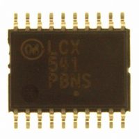
Manufacturer Part Number
MC74LCX541DTR2G
Description
IC BUFF/DVR TRI-ST 8BIT 20TSSOP
Manufacturer
ON Semiconductor
Series
74LCXr
Datasheet
1.MC74LCX541DTR2G.pdf
(8 pages)
Specifications of MC74LCX541DTR2G
Logic Type
Buffer/Line Driver, Non-Inverting
Number Of Elements
1
Number Of Bits Per Element
8
Current - Output High, Low
24mA, 24mA
Voltage - Supply
2 V ~ 3.6 V
Operating Temperature
-40°C ~ 85°C
Mounting Type
Surface Mount
Package / Case
20-TSSOP
Logic Family
LCX
Number Of Channels Per Chip
8
Polarity
Non-Inverting
Supply Voltage (max)
3.6 V
Supply Voltage (min)
2 V
Maximum Operating Temperature
+ 85 C
Mounting Style
SMD/SMT
High Level Output Current
- 24 mA
Low Level Output Current
24 mA
Maximum Power Dissipation
200 mW
Minimum Operating Temperature
- 40 C
Number Of Lines (input / Output)
8 / 3
Output Type
3-State
Propagation Delay Time
7.5 ns at 2.7 V, 6.5 ns at 3 V to 3.6 V
Lead Free Status / RoHS Status
Lead free / RoHS Compliant
Other names
MC74LCX541DTR2GOS
MC74LCX541DTR2GOS
MC74LCX541DTR2GOSTR
MC74LCX541DTR2GOS
MC74LCX541DTR2GOSTR
Available stocks
Company
Part Number
Manufacturer
Quantity
Price

Company:
Part Number:
MC74LCX541DTR2G
Manufacturer:
ONSemi
Quantity:
110 746


Maximum ratings are those values beyond which device damage can occur. Maximum ratings applied to the device are individual stress limit
values (not normal operating conditions) and are not valid simultaneously. If these limits are exceeded, device functional operation is not implied,
damage may occur and reliability may be affected.
1. Output in HIGH or LOW State. I
†For information on tape and reel specifications, including part orientation and tape sizes, please refer to our Tape and Reel Packaging
*This package is inherently Pb−Free.
MAXIMUM RATINGS
RECOMMENDED OPERATING CONDITIONS
Symbol
Symbol
ORDERING INFORMATION
Specifications Brochure, BRD8011/D.
MC74LCX541DW
MC74LCX541DWG
MC74LCX541DWR2
MC74LCX541DR2G
MC74LCX541DT
MC74LCX541DTR2
MC74LCX541MEL
V
V
V
I
I
I
I
I
T
V
V
V
I
I
I
I
T
Dt/DV
IK
OK
O
CC
GND
OH
OL
OH
OL
A
STG
CC
I
O
CC
I
O
DC Supply Voltage
DC Input Voltage
DC Output Voltage
DC Input Diode Current
DC Output Diode Current
DC Output Source/Sink Current
DC Supply Current Per Supply Pin
DC Ground Current Per Ground Pin
Storage Temperature Range
Supply Voltage
Input Voltage
Output Voltage
HIGH Level Output Current, V
LOW Level Output Current, V
HIGH Level Output Current, V
LOW Level Output Current, V
Operating Free−Air Temperature
Input Transition Rise or Fall Rate, V
Device
Parameter
O
absolute maximum rating must be observed.
CC
CC
Parameter
CC
CC
= 3.0 V − 3.6 V
= 2.7 V − 3.0 V
= 3.0 V − 3.6 V
= 2.7 V − 3.0 V
IN
from 0.8 V to 2.0 V, V
(HIGH or LOW State)
−0.5
Data Retention Only
http://onsemi.com
MC74LCX541
−0.5
−0.5
−0.5 to +7.0
−65 to +150
V
TSSOP−20*
TSSOP−20*
SOEIAJ−20
Value
O
(Pb−Free)
(Pb−Free)
SOIC−20
SOIC−20
SOIC−20
SOIC−20
Package
−50
−50
+50
V
100
100
V
50
Operating
3
O
(3−State)
I
V
CC
CC
+7.0
+7.0
+ 0.5
= 3.0 V
Min
−40
2.0
1.5
0
0
0
0
Output in 3−State
Condition
V
V
V
O
Note 1
I
O
< GND
Typ
< GND
3.3
3.3
> V
1000 Tape & Reel
1000 Tape & Reel
2000 Tape & Reel
2000 Tape & Reel
38 Units / Rail
38 Units / Rail
75 Units / Rail
CC
Shipping
Max
V
−24
−12
+85
†
3.6
3.6
5.5
5.5
24
12
10
CC
Unit
Unit
ns/V
mA
mA
mA
mA
mA
mA
mA
mA
mA
mA
V
V
V
V
V
V
V
C
C
Related parts for MC74LCX541DTR2G
Image
Part Number
Description
Manufacturer
Datasheet
Request
R

Part Number:
Description:
ON Semiconductor [VOLTAGE REGULATOR]
Manufacturer:
ON Semiconductor
Datasheet:
Part Number:
Description:
357-036-542-201 CARDEDGE 36POS DL .156 BLK LOPRO
Manufacturer:
ON Semiconductor
Datasheet:
Part Number:
Description:
357-036-542-201 CARDEDGE 36POS DL .156 BLK LOPRO
Manufacturer:
ON Semiconductor
Datasheet:
Part Number:
Description:
357-036-542-201 CARDEDGE 36POS DL .156 BLK LOPRO
Manufacturer:
ON Semiconductor
Datasheet:
Part Number:
Description:
357-036-542-201 CARDEDGE 36POS DL .156 BLK LOPRO
Manufacturer:
ON Semiconductor
Datasheet:
Part Number:
Description:
357-036-542-201 CARDEDGE 36POS DL .156 BLK LOPRO
Manufacturer:
ON Semiconductor
Datasheet:
Part Number:
Description:
357-036-542-201 CARDEDGE 36POS DL .156 BLK LOPRO
Manufacturer:
ON Semiconductor
Datasheet:
Part Number:
Description:
357-036-542-201 CARDEDGE 36POS DL .156 BLK LOPRO
Manufacturer:
ON Semiconductor
Datasheet:
Part Number:
Description:
357-036-542-201 CARDEDGE 36POS DL .156 BLK LOPRO
Manufacturer:
ON Semiconductor
Datasheet:
Part Number:
Description:
357-036-542-201 CARDEDGE 36POS DL .156 BLK LOPRO
Manufacturer:
ON Semiconductor
Datasheet:
Part Number:
Description:
357-036-542-201 CARDEDGE 36POS DL .156 BLK LOPRO
Manufacturer:
ON Semiconductor
Datasheet:
Part Number:
Description:
Manufacturer:
ON Semiconductor
Datasheet:
Part Number:
Description:
Manufacturer:
ON Semiconductor
Datasheet:
Part Number:
Description:
Manufacturer:
ON Semiconductor
Datasheet: