74LCXH2245MTC Fairchild Semiconductor, 74LCXH2245MTC Datasheet
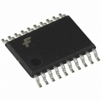
IC TXRX BIDIRECT BUSHOLD 20TSSOP

74LCXH2245MTC

Manufacturer Part Number
74LCXH2245MTC
Description
IC TXRX BIDIRECT BUSHOLD 20TSSOP
Manufacturer
Fairchild Semiconductor
Series
74LCXHr
Datasheet

Specifications of 74LCXH2245MTC

Logic Type
Transceiver, Non-Inverting
Number Of Elements
1
Number Of Bits Per Element
8
Current - Output High, Low
24mA, 24mA; 12mA, 12mA
Voltage - Supply
2 V ~ 3.6 V
Operating Temperature
-40°C ~ 85°C
Mounting Type
Surface Mount
Package / Case
20-TSSOP
Lead Free Status / RoHS Status
Lead free / RoHS Compliant

Available stocks

Company
Part Number
Manufacturer
Quantity
Price
Part Number:
74LCXH2245MTCX
Manufacturer:
Panasonic
Quantity:
17 590
Part Number:
74LCXH2245MTCX
Manufacturer:
FSC
Quantity:
2 030
© 2005 Fairchild Semiconductor Corporation
74LCXH2245WM
74LCXH2245SJ
74LCXH2245MSA
74LCXH2245MTC
74LCXH2245
Low Voltage Bidirectional Transceiver with Bushold
and 26: Series Resistors in B Outputs
General Description
The LCXH2245 contains eight non-inverting bidirectional
buffers with 3-STATE outputs and is intended for bus ori-
ented applications. The device is designed for low voltage
(2.5V and 3.3V) V
mines the direction of data flow through the device. The OE
input disables both the A and B ports by placing them in a
high impedance state. The 26
output helps reduce output overshoot and undershoot.
The LCXH2245 is fabricated with an advanced CMOS
technology to achieve high speed operation while maintain-
ing CMOS low power dissipation.
The LCXH2245 data inputs include active bushold circuitry,
eliminating the need for external pull-up resistors to hold
unused or floating data inputs at a valid logic level.
Ordering Code:
Devices also available in Tape and Reel. Specify by appending the suffix letter “X” to the ordering code.
Pb-Free package per JEDEC J-STD-020B.
Logic Symbol
Pin Descriptions
OE
T/R
A
B
GTO
Order Number
0
0
Pin Names
–A
–B
¥
7
7
is a trademark of Fairchild Semiconductor Corporation.
Output Enable Input
Transmit/Receive Input
Side A Inputs or 3-STATE Outputs (Bushold)
Side B Inputs or 3-STATE Outputs (Bushold)
Package Number
CC
applications. The T/R input deter-
MSA20
MTC20
M20D
M20B
:
series resistor in the B Port
Description
20-Lead Small Outline Integrated Circuit (SOIC), JEDEC MS-013, 0.300" Wide
Pb-Free 20-Lead Small Outline Package (SOP), EIAJ TYPE II, 5.3mm Wide
20-Lead Shrink Small Outline Package (SSOP), JEDEC MO-150, 5.3mm Wide
20-Lead Thin Shrink Small Outline Package (TSSOP), JEDEC MO-153, 4.4mm Wide
DS500409
Features
Connection Diagram
5V tolerant control inputs
2.3V–3.6V V
Bushold on inputs eliminates the need for external
pull-up/pull-down resistors
7.0 ns t
Power down high impedance outputs
r
Implements patented noise/EMI reduction circuitry
Latch-up performance exceeds 500 mA
Equivalent 26
ESD performance:
Human body model
Machine model
12 mA output drive B Port (V
Package Description
PD
max (V
CC
:
specifications provided
!
series resistor on B Port outputs
CC
200V
!
2000V
3.3V), 10
October 2000
Revised March 2005
CC
P
A I
3.0V)
CC
www.fairchildsemi.com
max

Related parts for 74LCXH2245MTC

74LCXH2245MTC Summary of contents

Page 1

... MSA20 20-Lead Shrink Small Outline Package (SSOP), JEDEC MO-150, 5.3mm Wide 74LCXH2245MTC MTC20 20-Lead Thin Shrink Small Outline Package (TSSOP), JEDEC MO-153, 4.4mm Wide Devices also available in Tape and Reel. Specify by appending the suffix letter “X” to the ordering code. ...

Page 2

Truth Table Inputs OE T HIGH Voltage Level L LOW Voltage Level X Immaterial Z High Impedance Logic Diagram www.fairchildsemi.com Outputs L Bus B – B Data to Bus A – ...

Page 3

Absolute Maximum Ratings Symbol Parameter V Supply Voltage CC V T/R, OE, I I/O Ports V DC Output Voltage Input Diode Current Output Diode Current Output Source/Sink Current ...

Page 4

DC Electrical Characteristics Symbol Parameter V LOW Level Output Voltage OL A Outputs V LOW Level Output Voltage OL B Outputs I Input Leakage Current I I Bushold Input Minimum I(HOLD) Drive Hold Current I Bushold Input Over-Drive I(OD) Current ...

Page 5

Dynamic Switching Characteristics Symbol Parameter V Quiet Output Dynamic Peak V OLP Quiet Output Dynamic Peak Quiet Output Dynamic Valley V OLV Quiet Output Dynamic Valley ...

Page 6

AC LOADING and WAVEFORMS FIGURE 1. AC Test Circuit (C Test PLH PZL PZH Waveform for Inverting and Non-Inverting Functions Propagation Delay. Pulse Width and t rec 3-STATE Output Low Enable ...

Page 7

Schematic Diagram Generic for LCXH Family (with Bushold) 7 www.fairchildsemi.com ...

Page 8

Physical Dimensions inches (millimeters) unless otherwise noted 20-Lead Small Outline Integrated Circuit (SOIC), JEDEC MS-013, 0.300" Wide www.fairchildsemi.com Package Number M20B 8 ...

Page 9

Physical Dimensions inches (millimeters) unless otherwise noted (Continued) Pb-Free 20-Lead Small Outline Package (SOP), EIAJ TYPE II, 5.3mm Wide Package Number M20D 9 www.fairchildsemi.com ...

Page 10

Physical Dimensions inches (millimeters) unless otherwise noted (Continued) 20-Lead Shrink Small Outline Package (SSOP), JEDEC MO-150, 5.3mm Wide www.fairchildsemi.com Package Number MSA20 10 ...

Page 11

Physical Dimensions inches (millimeters) unless otherwise noted (Continued) 20-Lead Thin Shrink Small Outline Package (TSSOP), JEDEC MO-153, 4.4mm Wide Fairchild does not assume any responsibility for use of any circuitry described, no circuit patent licenses are implied and Fairchild reserves ...

Related keywords