NLU2G07AMX1TCG ON Semiconductor, NLU2G07AMX1TCG Datasheet - Page 3
NLU2G07AMX1TCG
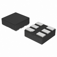
Manufacturer Part Number
NLU2G07AMX1TCG
Description
IC BUFF DL OP/DRAIN N-INV 6ULLGA
Manufacturer
ON Semiconductor
Datasheet
1.NLU2G07MUTCG.pdf
(8 pages)
Specifications of NLU2G07AMX1TCG
Logic Type
Buffer/Line Driver, Non-Inverting
Number Of Elements
2
Number Of Bits Per Element
1
Voltage - Supply
1.65 V ~ 5.5 V
Operating Temperature
-55°C ~ 125°C
Mounting Type
Surface Mount
Package / Case
6-ULLGA
Number Of Channels Per Chip
2
Polarity
Non-Inverting
Supply Voltage (max)
5.5 V
Supply Voltage (min)
1.65 V
Maximum Operating Temperature
+ 125 C
Mounting Style
Screw
Low Level Output Current
8 mA
Minimum Operating Temperature
- 55 C
Number Of Lines (input / Output)
2 / 2
Output Type
Open Drain
Propagation Delay Time
10.6 ns at 3 V to 3.6 V, 7.5 ns at 4.5 V to 5.5 V
Lead Free Status / RoHS Status
Lead free / RoHS Compliant
Current - Output High, Low
-
Lead Free Status / Rohs Status
Details
Available stocks
Company
Part Number
Manufacturer
Quantity
Price
Company:

Part Number:
NLU2G07AMX1TCG
Manufacturer:
ON Semiconductor
Quantity:
305


3. C
DC ELECTRICAL CHARACTERISTICS
AC ELECTRICAL CHARACTERISTICS
Symbol
Symbol
load. Average operating current can be obtained by the equation I
dynamic power consumption: P
I
I
C
V
t
t
C
V
I
V
LKG
OFF
I
PZL
PLZ
PD
CC
IN
OL
PD
IH
IN
IL
is defined as the value of the internal equivalent capacitance which is calculated from the dynamic operating current consumption without
Low-Level
Input Voltage
Low-Level
Input Voltage
Low-Level
Output Voltage
Z-State
Output
Leakage
Current
Input Leakage
Current
Power Off
Input Leakage
Current
Quiescent
Supply Current
Propagation Delay,
Input A to Output Y
Output Disable Time
Input Capacitance
Power Dissipation
Capacitance (Note 3)
Parameter
Parameter
V
I
V
I
I
V
V
GND
0 v V
0 v V
V
0 v V
OL
OL
OL
D
IN
IN
IN
OUT
OUT
Conditions
= C
= 50 mA
= 4 mA
= 8 mA
= V
= V
= V
= V
v 5.5 V
IN
IN
IN
PD
3.0 to 3.6
4.5 to 5.5
3.0 to 3.6
4.5 to 55
IH
IH
IH
,
v 5.5 V
v V
,
V
CC
or V
or V
5.0
• V
(V)
CC
or
CC
CC
IL
IL
(Input t
2
• f
in
R
C
R
C
R
C
R
C
R
C
R
C
2.3 to
2.3 to
r
V
1.65
1.65
+ I
0 to
L
L
L
L
L
L
L
L
L
L
L
L
(V)
5.5
5.5
2.0
3.0
4.5
3.0
4.5
5.5
5.5
5.5
= t
Condition
CC
0
= R
= 15 pF
= R
= 50 pF
= R
= 15 pF
= R
= 50 pF
= R
= 50 pF
= R
= 50 pF
CC
http://onsemi.com
f
Test
= 3.0 nS)
1
1
1
1
1
1
• V
= 50 W
= 50 W
= 50 W
= 50 W
= 50 W
= 50 W
NLU2G07
CC.
0.75 x
0.70 x
V
V
Min
CC
CC
3
CC(OPR)
T
A
Min
= 25 5C
Typ
0
0
0
= C
T
A
Typ
PD
5.0
7.5
3.8
5.3
7.5
5.3
4.0
18
= 25 5C
0.25 x
0.30 x
±0.25
Max
0.36
0.36
±0.1
0.25
V
V
0.1
0.1
0.1
1.0
• V
CC
CC
CC
Max
10.6
10.6
7.1
5.5
7.5
7.5
10
• f
0.75 x
0.70 x
in
V
V
Min
T
CC
CC
+ I
A
CC
= +855C
Min
T
. C
A
0.25 x
0.30 x
= +855C
Max
0.44
0.44
±2.5
±1.0
PD
V
V
0.1
0.1
0.1
2.5
10
CC
CC
is used to determine the no-load
Max
8.5
6.5
8.5
8.5
12
12
10
T
Min
A
Min
= -555C to
+1255C
T
to +1255C
A
= -555C
0.25 x
0.30 x
Max
0.52
0.52
±5.0
±1.0
V
V
0.1
0.1
0.1
5.0
Max
14.5
14.5
40
8.0
CC
CC
10
10
10
10
Unit
Unit
mA
mA
mA
mA
pF
pF
ns
ns
V
V
V
Related parts for NLU2G07AMX1TCG
Image
Part Number
Description
Manufacturer
Datasheet
Request
R

Part Number:
Description:
ON Semiconductor [VOLTAGE REGULATOR]
Manufacturer:
ON Semiconductor
Datasheet:
Part Number:
Description:
357-036-542-201 CARDEDGE 36POS DL .156 BLK LOPRO
Manufacturer:
ON Semiconductor
Datasheet:
Part Number:
Description:
357-036-542-201 CARDEDGE 36POS DL .156 BLK LOPRO
Manufacturer:
ON Semiconductor
Datasheet:
Part Number:
Description:
357-036-542-201 CARDEDGE 36POS DL .156 BLK LOPRO
Manufacturer:
ON Semiconductor
Datasheet:
Part Number:
Description:
357-036-542-201 CARDEDGE 36POS DL .156 BLK LOPRO
Manufacturer:
ON Semiconductor
Datasheet:
Part Number:
Description:
357-036-542-201 CARDEDGE 36POS DL .156 BLK LOPRO
Manufacturer:
ON Semiconductor
Datasheet:
Part Number:
Description:
357-036-542-201 CARDEDGE 36POS DL .156 BLK LOPRO
Manufacturer:
ON Semiconductor
Datasheet:
Part Number:
Description:
357-036-542-201 CARDEDGE 36POS DL .156 BLK LOPRO
Manufacturer:
ON Semiconductor
Datasheet:
Part Number:
Description:
357-036-542-201 CARDEDGE 36POS DL .156 BLK LOPRO
Manufacturer:
ON Semiconductor
Datasheet:
Part Number:
Description:
357-036-542-201 CARDEDGE 36POS DL .156 BLK LOPRO
Manufacturer:
ON Semiconductor
Datasheet:
Part Number:
Description:
357-036-542-201 CARDEDGE 36POS DL .156 BLK LOPRO
Manufacturer:
ON Semiconductor
Datasheet:
Part Number:
Description:
Manufacturer:
ON Semiconductor
Datasheet:
Part Number:
Description:
Manufacturer:
ON Semiconductor
Datasheet:
Part Number:
Description:
Manufacturer:
ON Semiconductor
Datasheet: