74ABT241CMSAX Fairchild Semiconductor, 74ABT241CMSAX Datasheet - Page 2
74ABT241CMSAX
Manufacturer Part Number
74ABT241CMSAX
Description
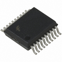
IC BUFF/DVR TRI-ST DUAL 20SSOP
Manufacturer
Fairchild Semiconductor
Series
74ABTr
Datasheet
1.74ABT241CMSA.pdf
(7 pages)
Specifications of 74ABT241CMSAX
Logic Type
Buffer/Line Driver, Non-Inverting
Number Of Elements
2
Number Of Bits Per Element
4
Current - Output High, Low
32mA, 64mA
Voltage - Supply
4.5 V ~ 5.5 V
Operating Temperature
-40°C ~ 85°C
Mounting Type
Surface Mount
Package / Case
20-SSOP
Lead Free Status / RoHS Status
Lead free / RoHS Compliant


www.fairchildsemi.com
V
V
V
V
V
I
I
I
V
I
I
I
I
I
I
I
I
I
I
Absolute Maximum Ratings
DC Electrical Characteristics
IH
BVI
IL
OZH
OZL
OS
CEX
ZZ
CCH
CCL
CCZ
CCT
CCD
Note 3: For 8 bits toggling, I
Note 4: Guaranteed, but not tested.
Storage Temperature
Ambient Temperature under Bias
Junction Temperature under Bias
V
Input Voltage (Note 2)
Input Current (Note 2)
Voltage Applied to Any Output
Current Applied to Output
DC Latchup Source Current
Over Voltage Latchup (I/O)
IH
IL
CD
OH
OL
ID
Symbol
CC
in the Disabled or
Power-Off State
in the HIGH State
in LOW State (Max)
(Over Comm Operating Range)
Pin Potential to Ground Pin
Input HIGH Voltage
Input LOW Voltage
Input Clamp Diode Voltage
Output HIGH Voltage
Output LOW Voltage
Input HIGH Current
Input HIGH Current Breakdown Test
Input LOW Current
Input Leakage Test
Output Leakage Current
Output Leakage Current
Output Short-Circuit Current
Output High Leakage Current
Bus Drainage Test
Power Supply Current
Power Supply Current
Power Supply Current
Additional I
Dynamic I
(Note 4)
CC
CC
CCD
/Input
Parameter
0.8 mA/MHz.
Outputs Enabled
Outputs 3-STATE
Outputs 3-STATE
No Load
twice the rated I
30 mA to 5.0 mA
65 C to 150 C
55 C to 125 C
55 C to 150 C
(Note 1)
0.5V to 7.0V
0.5V to 7.0V
0.5V to 5.5V
0.5V to V
4.75
Min
2.0
2.5
2.0
100
OL
500 mA
(mA)
10V
CC
Typ
2
Recommended Operating
Conditions
Note 1: Absolute maximum ratings are values beyond which the device
may be damaged or have its useful life impaired. Functional operation
under these conditions is not implied.
Note 2: Either voltage limit or current limit is sufficient to protect inputs.
Free Air Ambient Temperature
Supply Voltage
Minimum Input Edge Rate ( V/ t)
Data Input
Enable Input
Max
0.55
100
0.8
2.5
2.5
0.1
10
275
50
50
30
50
50
1.2
1
1
7
10
1
1
Units
MHz
mA/
mA
mA
mA
mA
V
V
V
V
V
V
V
A
A
A
A
A
A
A
A
A
A
0
0
Max
Max
Max
Max
Max
Max
Max
Max
Max
Max
V
Min
Min
Min
Min
0.0
0.0
CC
5.5V
5.5V
Recognized HIGH Signal
Recognized LOW Signal
I
I
I
I
V
V
V
V
V
I
All Other Pins Grounded
V
V
V
V
V
All Outputs HIGH
All Outputs LOW
OE
All Others at V
V
Enable Input V
Data Input V
All Others at V
Outputs Open
OE
One Bit Toggling, 50%
Duty Cycle
IN
OH
OH
OL
ID
IN
IN
IN
IN
IN
OUT
OUT
OUT
OUT
OUT
I
n
n
V
1.9 A
64 mA
2.7V (Note 4)
V
7.0V
0.5V (Note 4)
0.0V
CC
18 mA
V
GND, (Note 3)
3 mA
32 mA
CC
2.7V; OE
0.5V; OE
0.0V
V
5.5V; All Others GND
CC
Conditions
CC
40 C to 85 C
;
2.1V
4.5V to 5.5V
I
CC
CC
I
V
50 mV/ns
20 mV/ns
n
n
CC
or Ground
V
or Ground
CC
2.0V
2.0V
2.1V
2.1V
Related parts for 74ABT241CMSAX
Image
Part Number
Description
Manufacturer
Datasheet
Request
R

Part Number:
Description:
Octal Buffer/Line Driver with 3-STATE Outputs
Manufacturer:
Fairchild Semiconductor
Datasheet:

Part Number:
Description:
IC TRANSCVR TRI-ST 8BIT 20SOIC
Manufacturer:
Fairchild Semiconductor
Datasheet:

Part Number:
Description:
IC BUFF/DVR TRI-ST 8BIT 20SOIC
Manufacturer:
Fairchild Semiconductor
Datasheet:

Part Number:
Description:
IC BUFF TRI-ST QD N-INV 14SOICN
Manufacturer:
NXP Semiconductors
Datasheet:

Part Number:
Description:
IC BUFF/DVR TRI-ST 8BIT 20SOIC
Manufacturer:
NXP Semiconductors
Datasheet:
Part Number:
Description:
IC BUFF/DVR TRI-ST DUAL 20SOIC
Manufacturer:
NXP Semiconductors
Datasheet:

Part Number:
Description:
IC BUFF/DVR TRI-ST DUAL 20SOIC
Manufacturer:
Fairchild Semiconductor
Datasheet:

Part Number:
Description:
IC BUFF/DVR TRI-ST 8BIT 20DIP
Manufacturer:
NXP Semiconductors
Datasheet:

Part Number:
Description:
IC BUFF TRI-ST QD N-INV 14TSSOP
Manufacturer:
Fairchild Semiconductor

Part Number:
Description:
IC BUFF TRI-ST QD N-INV 14SOIC
Manufacturer:
Fairchild Semiconductor

Part Number:
Description:
IC BUFF/DVR TRI-ST DUAL 20TSSOP
Manufacturer:
Fairchild Semiconductor
Part Number:
Description:
IC BUFF/DVR TRI-ST DUAL 20TSSOP
Manufacturer:
Fairchild Semiconductor
Datasheet:

Part Number:
Description:
IC BUFF TRI-ST QD N-INV 14SOP
Manufacturer:
Fairchild Semiconductor
Datasheet:

Part Number:
Description:
IC BUFF/DVR TRI-ST DUAL 20SOP
Manufacturer:
Fairchild Semiconductor
Part Number:
Description:
IC TRANSCVR TRI-ST 8BIT 20SOIC
Manufacturer:
Fairchild Semiconductor
Datasheet: