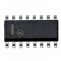
MC74AC161DR2G ON Semiconductor, MC74AC161DR2G Datasheet - Page 2

MC74AC161DR2G
Manufacturer Part Number
MC74AC161DR2G
Description
IC COUNTER SYNC BINARY 16-SOIC
Manufacturer
ON Semiconductor
Series
74ACr
Type
Binaryr
Datasheet
1.MC74AC161DG.pdf
(15 pages)
Specifications of MC74AC161DR2G
Logic Type
Binary Counter
Direction
Up
Number Of Elements
1
Number Of Bits Per Element
4
Reset
Asynchronous
Timing
Synchronous
Count Rate
167MHz
Trigger Type
Positive Edge
Voltage - Supply
2 V ~ 6 V
Operating Temperature
-40°C ~ 85°C
Mounting Type
Surface Mount
Package / Case
16-SOIC (3.9mm Width)
Technology
CMOS
Number Of Elements
1
Number Of Bits
4
Logic Family
AC
Logical Function
Counter
Operating Supply Voltage (typ)
5V
Package Type
SOIC
Propagation Delay Time
17.5ns
Operating Temp Range
-40C to 85C
Operating Supply Voltage (min)
2V
Operating Supply Voltage (max)
6V
Operating Temperature Classification
Industrial
Mounting
Surface Mount
Pin Count
16
Lead Free Status / RoHS Status
Lead free / RoHS Compliant
Available stocks
Company
Part Number
Manufacturer
Quantity
Price
Company:
Part Number:
MC74AC161DR2G
Manufacturer:
ON Semiconductor
Quantity:
1 600
Part Number:
MC74AC161DR2G
Manufacturer:
ON/安森美
Quantity:
20 000
count modulo−16 binary sequence. From state 15 (HHHH)
they increment to state 0 (LLLL). The clock inputs of all
flip−flops are driven in parallel through a clock buffer. Thus
all changes of the Q outputs (except due to Master Reset of
the ′161) occur as a result of, and synchronous with, the
LOW−to−HIGH transition of the CP input signal. The
circuits have four fundamental modes of operation, in order
of precedence: asynchronous reset (′161), synchronous reset
(′163), parallel load, count−up and hold. Five control inputs
− Master Reset (MR, ′161), Synchronous Reset (SR, ′163),
Parallel Enable (PE), Count Enable Parallel (CEP) and
Count Enable Trickle (CET) − determine the mode of
MODE SELECT TABLE
*For ′163 only
H = HIGH Voltage Level
L = LOW Voltage Level
X = Immaterial
*SR
The MC74AC161/ACT161 and MC74AC163/ACT163
H
H
H
H
L
PE
X
H
H
H
L
FUNCTIONAL DESCRIPTION
CET
Figure 2. Logic Symbol
X
X
H
X
L
CEP
CET
CP
PE P
*R Q
*MR for ′161
*SR for ′163
CEP
X
X
H
X
L
0
0
P
Q
1
1
Action on the Rising
Clock Edge ( )
Reset (Clear)
Load (P
Count (Increment)
No Change (Hold)
No Change (Hold)
Q
P
2
2
P
Q
3
3
TC
n
→ Q
n
)
http://onsemi.com
2
operation, as shown in the Mode Select Table. A LOW
signal on MR overrides all other inputs and asynchronously
forces all outputs LOW. A LOW signal on SR overrides
counting and parallel loading and allows all outputs to go
LOW on the next rising edge of CP. A LOW signal on PE
overrides counting and allows information on the Parallel
Data (P
rising edge of CP. With PE and MR (′161) or SR (′163)
HIGH, CEP and CET permit counting when both are HIGH.
Conversely, a LOW signal on either CEP or CET inhibits
counting.
D−type edge−triggered flip−flops and changing the SR, PE,
CEP and CET inputs when the CP is in either state does not
cause errors, provided that the recommended setup and hold
times, with respect to the rising edge of CP, are observed.
HIGH and counter is in state 15. To implement synchronous
multistage counters, the TC outputs can be used with the
CEP and CET inputs in two different ways. Please refer to
the MC74AC568 data sheet. The TC output is subject to
decoding spikes due to internal race conditions and is
therefore not recommended for use as a clock or
asynchronous reset for flip−flops, counters or registers.
Logic Equations:
The MC74AC161/ACT161 and MC74AC163/ACT163 use
The Terminal Count (TC) output is HIGH when CET is
n
) inputs to be loaded into the flip−flops on the next
Count Enable = CEP
TC = Q
Figure 3. State Diagram
15
14
13
12
0
0
11
1
•
Q
1
•
Q
10
2
2
•
Q
3
3
9
•
CET
•
CET
4
5
6
7
8
•
PE


