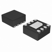
MC100EP32MNR4G ON Semiconductor, MC100EP32MNR4G Datasheet - Page 3

MC100EP32MNR4G
Manufacturer Part Number
MC100EP32MNR4G
Description
IC DIVIDER BY4 ECL CLK IN 8-DFN
Manufacturer
ON Semiconductor
Series
100EPr
Datasheet
1.MC100EP32DTG.pdf
(11 pages)
Specifications of MC100EP32MNR4G
Logic Type
Divide-by-2
Number Of Elements
1
Number Of Bits Per Element
1
Reset
Asynchronous
Count Rate
4GHz
Trigger Type
Positive, Negative
Voltage - Supply
3 V ~ 5.5 V
Operating Temperature
-40°C ~ 85°C
Mounting Type
Surface Mount
Package / Case
8-TFDFN Exposed Pad
Lead Free Status / RoHS Status
Lead free / RoHS Compliant
Direction
-
Timing
-
Lead Free Status / Rohs Status
Compliant
Other names
MC100EP32MNR4G
MC100EP32MNR4GOSTR
MC100EP32MNR4GOSTR
Available stocks
Company
Part Number
Manufacturer
Quantity
Price
Part Number:
MC100EP32MNR4G
Manufacturer:
ON/安森美
Quantity:
20 000
Stresses exceeding Maximum Ratings may damage the device. Maximum Ratings are stress ratings only. Functional operation above the
Recommended Operating Conditions is not implied. Extended exposure to stresses above the Recommended Operating Conditions may affect
device reliability.
2. JEDEC standard multilayer board − 2S2P (2 signal, 2 power)
NOTE: Device will meet the specifications after thermal equilibrium has been established when mounted in a test socket or printed circuit
3. Input and output parameters vary 1:1 with V
4. All loading with 50 W to V
5. V
Table 4. MAXIMUM RATINGS
Symbol
Table 5. 10EP DC CHARACTERISTICS, PECL
Symbol
V
V
V
I
I
T
T
q
q
q
q
q
T
q
I
V
V
V
V
V
V
I
I
out
BB
EE
IH
IL
A
stg
JA
JC
JA
JC
JA
sol
JC
CC
EE
I
OH
OL
IH
IL
BB
IHCMR
input signal.
IHCMR
board with maintained transverse airflow greater than 500 lfpm. Electrical parameters are guaranteed only over the declared
operating temperature range. Functional operation of the device exceeding these conditions is not implied. Device specification limit
values are applied individually under normal operating conditions and not valid simultaneously.
min varies 1:1 with V
PECL Mode Power Supply
NECL Mode Power Supply
PECL Mode Input Voltage
NECL Mode Input Voltage
Output Current
V
Operating Temperature Range
Storage Temperature Range
Thermal Resistance (Junction−to−Ambient)
Thermal Resistance (Junction−to−Case)
Thermal Resistance (Junction−to−Ambient)
Thermal Resistance (Junction−to−Case)
Thermal Resistance (Junction−to−Ambient)
Wave Solder
Thermal Resistance (Junction−to−Case)
Power Supply Current
Output HIGH Voltage (Note 4)
Output LOW Voltage (Note 4)
Input HIGH Voltage (Single−Ended)
Input LOW Voltage (Single−Ended)
Output Voltage Reference
Input HIGH Voltage Common Mode
Range (Differential Configuration) (Note 5)
Input HIGH Current
Input LOW Current
BB
Sink/Source
Characteristic
CC
Parameter
EE
− 2.0 V.
, V
IHCMR
max varies 1:1 with V
CC
. V
Pb−Free
EE
V
can vary +0.3 V to −2.2 V.
Pb
CC
2165
1365
2090
1365
1790
Min
http://onsemi.com
2.0
0.5
23
= 3.3 V, V
V
V
V
V
Continuous
Surge
0 lfpm
500 lfpm
Standard Board
0 lfpm
500 lfpm
Standard Board
0 lfpm
500 lfpm
<2 to 3 sec @ 248°C
<2 to 3 sec @ 260°C
(Note 2)
EE
CC
EE
CC
CC
Condition 1
−40°C
= 0 V
= 0 V
. The V
= 0 V
= 0 V
2290
1490
1890
Typ
30
3
EE
IHCMR
= 0 V (Note 3)
2415
1615
2415
1690
1990
Max
150
3.3
40
range is referenced to the most positive side of the differential
2230
1430
2155
1430
1855
Min
2.0
0.5
23
V
V
SOIC−8
SOIC−8
SOIC−8
TSSOP−8
TSSOP−8
TSSOP−8
DFN8
DFN8
DFN8
I
I
v V
w V
Condition 2
25°C
2355
1555
1955
CC
EE
Typ
30
2480
1680
2480
1755
2055
Max
150
3.3
40
2290
1490
2215
1490
1915
Min
2.0
0.5
23
−65 to +150
−40 to +85
41 to 44
41 to 44
35 to 40
Rating
± 0.5
85°C
2415
1615
2015
100
190
130
185
140
129
265
265
Typ
−6
−6
50
84
30
6
6
2540
1740
2540
1815
2115
Max
150
3.3
40
°C/W
°C/W
°C/W
°C/W
°C/W
°C/W
°C/W
°C/W
°C/W
Unit
mA
mA
mA
Unit
°C
°C
°C
mA
mV
mV
mV
mV
mV
mA
mA
V
V
V
V
V


