CY7C4261V-15JXC Cypress Semiconductor Corp, CY7C4261V-15JXC Datasheet - Page 15
CY7C4261V-15JXC
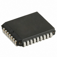
Manufacturer Part Number
CY7C4261V-15JXC
Description
IC SYNC FIFO MEM 16KX9 32-PLCC
Manufacturer
Cypress Semiconductor Corp
Series
CY7Cr
Datasheet
1.CY7C4281V-10JXC.pdf
(22 pages)
Specifications of CY7C4261V-15JXC
Access Time
10ns
Memory Size
144K (16K x 9)
Package / Case
32-PLCC
Function
Synchronous
Data Rate
100MHz
Voltage - Supply
3.3V
Operating Temperature
-40°C ~ 85°C
Mounting Type
Surface Mount
Number Of Circuits
2
Data Bus Width
9 bit
Bus Direction
Unidirectional
Timing Type
Synchronous
Organization
16 K x 9
Maximum Clock Frequency
66.7 MHz
Supply Voltage (max)
3.6 V
Supply Voltage (min)
3 V
Maximum Operating Current
25 mA
Maximum Operating Temperature
+ 70 C
Minimum Operating Temperature
0 C
Mounting Style
SMD/SMT
Lead Free Status / RoHS Status
Lead free / RoHS Compliant
Lead Free Status / RoHS Status
Lead free / RoHS Compliant, Lead free / RoHS Compliant
Available stocks
Company
Part Number
Manufacturer
Quantity
Price
Company:

Part Number:
CY7C4261V-15JXC
Manufacturer:
Cypress Semiconductor Corp
Quantity:
10 000


Switching Waveforms
Full Flag Timing
Programmable Almost Empty Flag Timing
Notes
Document #: 38-06013 Rev. *F
20. t
21. t
22. PAE offset = n.
23. If a read is performed on this rising edge of the read clock, there will be Empty + (n1) words in the FIFO when PAE goes LOW.
(if applicable)
(if applicable)
between the rising edge of RCLK and the rising edge of WCLK is less than t
WCLK and the rising RCLK is less than t
SKEW1
SKEW2
WEN2
WEN2
Q
D
WCLK
WEN1
REN1,
WCLK
RCLK
WEN1
REN1,
REN2
RCLK
0
0
REN2
PAE
–Q
–D
OE
FF
is the minimum time between a rising RCLK edge and a rising WCLK edge to guarantee that FF will go HIGH during the current clock cycle. If the time
is the minimum time between a rising WCLK and a rising RCLK edge for PAE to change state during that clock cycle. If the time between the edge of
8
8
Data In Output Register
t
t
LOW
SKEW1
CLKH
[20]
t
ENS
No Write
(continued)
t
SKEW2
SKEW2
t
WFF
t
t
A
ENH
t
t
ENS
ENS
, then PAE may not change state until the next RCLK.
[21]
t
t
ENH
ENH
t
CLKL
t
DS
t
PAE
22
SKEW1
Data Write
, then FF may not change state until the next WCLK rising edge.
Data Read
t
ENS
t
WFF
t
SKEW1
N + 1 WORDS
t
[20]
ENS
IN FIFO
t
ENS
CY7C4261V/CY7C4271V
CY7C4281V/CY7C4291V
No Write
t
ENH
t
WFF
t
t
A
ENH
Next Data Read
23
Data Write
t
PAE
Page 15 of 22
[+] Feedback
Related parts for CY7C4261V-15JXC
Image
Part Number
Description
Manufacturer
Datasheet
Request
R

Part Number:
Description:
IC DEEP SYNC FIFO 16KX9 32-PLCC
Manufacturer:
Cypress Semiconductor Corp
Datasheet:

Part Number:
Description:
IC,FIFO,16KX9,SYNCHRONOUS,CMOS,LDCC,32PIN,PLASTIC
Manufacturer:
Cypress Semiconductor Corp
Datasheet:

Part Number:
Description:
Manufacturer:
Cypress Semiconductor Corp
Datasheet:
Part Number:
Description:
IC DEEP SYNC FIFO 16KX9 32-PLCC
Manufacturer:
Cypress Semiconductor Corp
Datasheet:
Part Number:
Description:
IC DEEP SYNC FIFO 16KX9 32-PLCC
Manufacturer:
Cypress Semiconductor Corp
Datasheet:
Part Number:
Description:
Manufacturer:
Cypress Semiconductor Corp
Datasheet:
Part Number:
Description:
Manufacturer:
Cypress Semiconductor Corp
Datasheet:

Part Number:
Description:
Manufacturer:
Cypress Semiconductor Corp
Datasheet:
Part Number:
Description:
IC DEEP SYNC FIFO 16KX9 32-PLCC
Manufacturer:
Cypress Semiconductor Corp
Datasheet:
Part Number:
Description:
IC SYNC FIFO MEM 16KX9 32-PLCC
Manufacturer:
Cypress Semiconductor Corp
Datasheet:
Part Number:
Description:
IC,FIFO,16KX9,SYNCHRONOUS,CMOS,LDCC,32PIN,PLASTIC
Manufacturer:
Cypress Semiconductor Corp
Datasheet:
Part Number:
Description:
Manufacturer:
Cypress Semiconductor Corp
Datasheet:
Part Number:
Description:
Manufacturer:
Cypress Semiconductor Corp
Datasheet:
Part Number:
Description:
Manufacturer:
Cypress Semiconductor Corp
Datasheet: