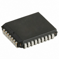
CY7C433-15JXC Cypress Semiconductor Corp, CY7C433-15JXC Datasheet

CY7C433-15JXC
Specifications of CY7C433-15JXC
Available stocks
Related parts for CY7C433-15JXC
CY7C433-15JXC Summary of contents
Page 1
... Read enable (R) and write enable (W) must both be HIGH during retransmit, and then R is used to access the data. The CY7C419, CY7C420, CY7C421, CY7C424, CY7C425, CY7C428, CY7C429, CY7C432, and CY7C433 are fabricated using an advanced 0.65-micron P-well CMOS technology. Input ESD protection is greater than 2000V and latch-up is prevented by careful layout and guard rings. • ...
Page 2
Pin Configurations Figure 1. 32-Pin PLCC/LCC Figure 2. 28-Pin DIP Table 1. Selection Guide –10 Frequency (MHz) 50 Maximum Access Time (ns (mA) 35 CC1 Document #: 38-06001 Rev. *C Figure 3. 32-PIn TQFP –15 ...
Page 3
Maximum Rating Exceeding maximum ratings may impair the useful life of the device. These user guidelines are not tested. Storage Temperature ................................. –65 Ambient Temperature with Power Applied.. –55 Supply Voltage to Ground Potential................–0.5V to +7.0V DC Voltage Applied to ...
Page 4
Electrical Characteristics Over the Operating Range Parameter Description I Operating Current OUT Operating Current V CC1 CC I OUT MHz I Standby Current All Inputs = SB1 V IH ...
Page 5
Switching Characteristics Over the Operating Range Parameter Description t Read Cycle Time RC t Access Time A t Read Recovery Time RR t Read Pulse Width PR [6,9] t Read LOW to Low Z LZR [9,10] t Data Valid After ...
Page 6
Switching Characteristics Over the Operating Range Parameter Description t Read Cycle Time RC t Access Time A t Read Recovery Time RR t Read Pulse Width PR [6,9] t Read LOW to Low Z LZR [9,10] t Data Valid After ...
Page 7
Switching Waveforms LZR Q – – [11 HALF FULL Notes 11. W and R ≥ V around the rising ...
Page 8
Switching Waveforms (continued) Figure 7. Last Write to First Read Full Flag LAST WRITE WFF FF Figure 8. Last Read to First Write Empty Flag LAST READ REF VALID DATA OUT ...
Page 9
Switching Waveforms (continued) Figure 10. Empty Flag and Read Data Flow-through Mode DATA DATA OUT Figure 11. Full Flag and Write Data Flow-through Mode DATA DATA OUT DATA VALID Document ...
Page 10
Switching Waveforms (continued) WRITE TO LAST PHYSICAL LOCATION OF DEVICE XOL [15 – READ FROM LAST PHYSICAL LOCATION OF DEVICE XOL [15 ...
Page 11
Architecture The CY7C419, CY7C420/1, CY7C424/5, CY7C432/3 FIFOs consist of an array of 256, 512, 1024, 2048, 4096 words of 9 bits each (implemented by an array of dual-port RAM cells), a read pointer, a write pointer, control signals (W, R, ...
Page 12
FIFO, with a signal that is asynchronous to the read signal. The (internal) state machine in the FIFO goes from empty to empty+1. However, it does this asynchronously with respect to the read signal, so that the effective ...
Page 13
Ordering Information Speed (ns) Ordering Code 10 CY7C421–10AC CY7C421–10JC CY7C421–10JXC CY7C421–10PC CY7C421–10VC 15 CY7C421–15AC CY7C421–15AXC CY7C421–15JC CY7C421–15JI CY7C421–15VI 20 CY7C421–20JC CY7C421–20JXC CY7C421–20PC CY7C421–20VC CY7C421–20VXC CY7C421–20JI CY7C421–20JXI 25 CY7C421–25JC CY7C421–25PC CY7C421–25VC CY7C421–25JI CY7C421–25PI 30 CY7C421–30JC CY7C421–30PC CY7C421–30JI 40 CY7C421–40JC CY7C421–40PC CY7C421–40VC ...
Page 14
Package Diagrams Figure 14. 32-Pin Thin Plastic Quad Flat Pack A32 (51-85063) Figure 15. 32-Pin Plastic Leaded Chip Carrier J65 (51-85002) Document #: 38-06001 Rev. *C CY7C419/21/25/29/33 51-85063-*B 51-85002-*B Page [+] Feedback ...
Page 15
Package Diagrams (continued) Figure 16. 28-Pin (300-Mil) PDIP P21 (51-85014 1.345[34.16] 1.385[35.18] 0.140[3.55] 0.190[4.82] 0.115[2.92] 0.160[4.06] 0.090[2.28] 0.110[2.79] LEAD END OPTION (LEAD #1, 14, 15 & 28) Document #: 38-06001 Rev. *C SEE LEAD END OPTION 1 0.260[6.60] ...
Page 16
Package Diagrams (continued) Figure 17. 28-Pin (300-Mil) Molded SOJ V21(51-85031) Document #: 38-06001 Rev. *C CY7C419/21/25/29/33 51-85031-*C Page [+] Feedback ...
Page 17
... Document History Page Document Title: CY7C419, CY7C421, CY7C425, CY7C429, CY7C433, 256/512/1K/2K/4Kx9 Asynchronous FIFO Document Number: 38-06001 Orig. of Rev. ECN No. Change ** 106462 SZV *A 122332 RBI *B 383597 PCX *C 2623658 VKN/PYRS Sales, Solutions and Legal Information Worldwide Sales and Design Support Cypress maintains a worldwide network of offices, solution centers, manufacturer’s representatives, and distributors. To find the office closest to you, visit us at cypress ...


