74AC374MTR STMicroelectronics, 74AC374MTR Datasheet
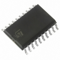
IC FLIP FLOP OCTAL D 20-SOIC

74AC374MTR

Manufacturer Part Number
74AC374MTR
Description
IC FLIP FLOP OCTAL D 20-SOIC
Manufacturer
STMicroelectronics
Series
74ACr
Type
D-Type Busr
Datasheet

Specifications of 74AC374MTR

Function
Standard
Output Type
Tri-State Non Inverted
Number Of Elements
1
Number Of Bits Per Element
8
Frequency - Clock
270MHz
Delay Time - Propagation
5ns
Trigger Type
Positive Edge
Current - Output High, Low
24mA, 24mA
Voltage - Supply
2 V ~ 6 V
Operating Temperature
-55°C ~ 125°C
Mounting Type
Surface Mount
Package / Case
20-SOIC (7.5mm Width)
Logic Family
AC
Technology
CMOS
Number Of Bits
8
Number Of Elements
1
Clock-edge Trigger Type
Positive-Edge
Polarity
Non-Inverting
Operating Supply Voltage (typ)
2.5/3.3/5V
Package Type
SOP
Propagation Delay Time
16.5ns
Low Level Output Current
24mA
High Level Output Current
-24mA
Frequency (max)
100MHz
Operating Supply Voltage (min)
2V
Operating Supply Voltage (max)
6V
Operating Temp Range
-55C to 125C
Operating Temperature Classification
Military
Mounting
Surface Mount
Pin Count
20
Lead Free Status / RoHS Status
Contains lead / RoHS non-compliant
Other names
497-1027-2

Available stocks

Company
Part Number
Manufacturer
Quantity
Price
Part Number:
74AC374MTR
Manufacturer:
ST
0
DESCRIPTION
The 74AC374 is an advanced high-speed CMOS
OCTAL D-TYPE FLIP-FLOP with 3 STATE
OUTPUT NON INVERTING fabricated with
sub-micron silicon gate and double-layer metal
wiring C
These 8 bit D-Type Flip-Flop are controlled by a
clock input (CK) and an output enable input (OE).
On the positive transition of the clock, the Q
outputs will be set to the logic that were setup at
PIN CONNECTION AND IEC LOGIC SYMBOLS
April 2001
HIGH SPEED:
f
LOW POWER DISSIPATION:
I
HIGH NOISE IMMUNITY:
V
50 TRANSMISSION LINE DRIVING
CAPABILITY
SYMMETRICAL OUTPUT IMPEDANCE:
|I
BALANCED PROPAGATION DELAYS:
t
OPERATING VOLTAGE RANGE:
V
PIN AND FUNCTION COMPATIBLE WITH
74 SERIES 374
IMPROVED LATCH-UP IMMUNITY
MAX
CC
PLH
OH
NIH
CC
= 4 A(MAX.) at T
| = I
(OPR) = 2V to 6V
2
= 270MHz (TYP.) at V
= V
MOS technology.
t
PHL
OL
NIL
= 24mA (MIN)
= 28 % V
A
CC
=25°C
(MIN.)
WITH 3 STATE OUTPUTS (NON INVERTED)
CC
= 5V
ORDER CODES
the D inputs.
While the (OE) input is low, the 8 outputs will be in
a normal logic state (high or low logic level); while
OE is in high level, the outputs will be in a high
impedance state.
The output control does not affect the internal
operation of flip-flops; that is, the old data can be
retained or the new data can be entered even
while the outputs are off.
All inputs and outputs are equipped with
protection circuits against static discharge, giving
them 2KV ESD immunity and transient excess
voltage.
OCTAL D-TYPE FLIP-FLOP
PACKAGE
TSSOP
SOP
DIP
DIP
74AC374M
74AC374B
TUBE
SOP
74AC374
74AC374MTR
74AC374TTR
TSSOP
T & R
1/11

Related parts for 74AC374MTR

74AC374MTR Summary of contents

Page 1

... All inputs and outputs are equipped with protection circuits against static discharge, giving them 2KV ESD immunity and transient excess voltage. 74AC374 SOP TSSOP TUBE T & R 74AC374B 74AC374M 74AC374MTR 74AC374TTR 1/11 ...

Page 2

INPUT AND OUTPUT EQUIVALENT CIRCUIT TRUTH TABLE Don’t Care Z : High Impedance LOGIC DIAGRAM This logic diagram has not be used to estimate propagation delays 2/11 PIN DESCRIPTION PIN No 1 ...

Page 3

ABSOLUTE MAXIMUM RATINGS Symbol V Supply Voltage Input Voltage Output Voltage Input Diode Current Output Diode Current Output Current ...

Page 4

DC SPECIFICATIONS Symbol Parameter V (V) V High Level Input 3.0 IH Voltage 4.5 5.5 V Low Level Input 3.0 IL Voltage 4.5 5.5 V High Level Output 3.0 OH Voltage 4.5 5.5 3.0 4.5 5.5 V Low Level ...

Page 5

AC ELECTRICAL CHARACTERISTICS (C Symbol Parameter V ( Propagation Delay 3.3 PLH PHL Time 5 Output Enable 3.3 PZL PZH Time 5 Output Disable 3.3 PLZ PHZ Time 5.0 t CLOCK ...

Page 6

TEST CIRCUIT PLH PHL PZL PLZ PZH PHZ C = 50pF or equivalent (includes jig and probe capacitance 500 or equivalent ...

Page 7

WAVEFORM 2: OUTPUT ENABLE AND DISABLE TIMES (f=1MHz; 50% duty cycle) WAVEFORM 3: PULSE WIDTH (f=1MHz; 50% duty cycle) 74AC374 7/11 ...

Page 8

Plastic DIP-20 (0.25) MECHANICAL DATA DIM. MIN. a1 0.254 B 1. 8/11 mm TYP. MAX. MIN. 0.010 1.65 0.055 0.45 0.25 25.4 8.5 2.54 22.86 7.1 3.93 3.3 1.34 ...

Page 9

SO-20 MECHANICAL DATA mm DIM. MIN. TYP 0. 0.35 b1 0. 12.60 E 10.00 e 1.27 e3 11.43 F 7. inch MAX. MIN. TYP. 2.65 0.20 0.004 2.45 ...

Page 10

DIM. MIN 0.05 A2 0.85 b 0.19 c 0.09 D 6.4 E 6. PIN 1 IDENTIFICATION 1 10/11 TSSOP20 MECHANICAL DATA mm TYP. MAX. 1.1 ...

Page 11

... No license is granted by implication or otherwise under any patent or patent rights of STMicroelectronics. Specifications mentioned in this publication are subject to change without notice. This publication supersedes and replaces all information previously supplied ...

Related keywords