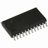
74ACT825SC Fairchild Semiconductor, 74ACT825SC Datasheet - Page 2

74ACT825SC
Manufacturer Part Number
74ACT825SC
Description
IC FLIP FLOP D-TYPE 8-BIT 24SOIC
Manufacturer
Fairchild Semiconductor
Series
74ACTr
Type
D-Type Busr
Datasheet
1.74ACT825SC.pdf
(7 pages)
Specifications of 74ACT825SC
Function
Master Reset
Output Type
Tri-State Non Inverted
Number Of Elements
1
Number Of Bits Per Element
8
Frequency - Clock
158MHz
Delay Time - Propagation
5.5ns
Trigger Type
Positive Edge
Current - Output High, Low
24mA, 24mA
Voltage - Supply
4.5 V ~ 5.5 V
Operating Temperature
-40°C ~ 85°C
Mounting Type
Surface Mount
Package / Case
24-SOIC (7.5mm Width)
Logic Family
ACT
Technology
CMOS
Number Of Bits
8
Number Of Elements
1
Clock-edge Trigger Type
Positive-Edge
Polarity
Non-Inverting
Operating Supply Voltage (typ)
5V
Package Type
SOIC W
Propagation Delay Time
12ns
Low Level Output Current
24mA
High Level Output Current
-24mA
Frequency (max)
109MHz
Operating Supply Voltage (min)
4.5V
Operating Supply Voltage (max)
5.5V
Operating Temp Range
-40C to 85C
Operating Temperature Classification
Industrial
Mounting
Surface Mount
Pin Count
24
Lead Free Status / RoHS Status
Lead free / RoHS Compliant
www.fairchildsemi.com
Functional Description
The ACT825 consists of eight D-type edge-triggered flip-
flops. These devices have 3-STATE outputs for bus sys-
tems, organized in a broadside pinning. In addition to the
clock and output enable pins, the buffered clock (CP) and
buffered Output Enable (OE) are common to all flip-flops.
The flip-flops will store the state of their individual D inputs
that meet the setup and hold time requirements on the
LOW-to-HIGH CP transition. With OE
LOW, the contents of the flip-flops are available at the out-
puts. When one of OE
go to the high impedance state.
Function Table
H
L
X
Z
NC
Logic Diagram
Please note that this diagram is provided only for the understanding of logic operations and should not be used to estimate propagation delays.
LOW Voltage Level
High Impedance
HIGH Voltage Level
Immaterial
LOW-to-HIGH Transition
No Change
OE
H
H
H
H
H
H
L
L
L
L
1
, OE
CLR
X
X
H
H
H
H
H
H
L
L
2
or OE
Inputs
EN
3
H
H
X
X
L
L
L
L
L
L
is HIGH, the outputs
1
, OE
CP
2
X
X
X
X
and OE
D
3
H
H
H
L
X
X
X
X
L
L
n
2
Operation of the OE input does not affect the state of the
flip-flops. The ACT825 has Clear (CLR) and Clock Enable
(EN) pins. These pins are ideal for parity bus interfacing in
high performance systems.
When CLR is LOW and OE is LOW, the outputs are LOW.
When CLR is HIGH, data can be entered into the flip-flops.
When EN is LOW, data on the inputs is transferred to the
outputs on the LOW-to-HIGH clock transition. When EN is
HIGH, the outputs do not change state, regardless of the
data or clock input transitions.
Internal
NC
NC
Q
H
H
H
L
L
L
L
L
Output
NC
O
H
Z
Z
Z
L
Z
Z
Z
L
High-Z
High-Z
Clear
Clear
Hold
Hold
Load
Load
Load
Load
Function


