MC74VHCT574ADTG ON Semiconductor, MC74VHCT574ADTG Datasheet
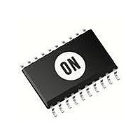
IC FLIP FLOP OCT D 3ST 20-TSSOP

MC74VHCT574ADTG

Manufacturer Part Number
MC74VHCT574ADTG
Description
IC FLIP FLOP OCT D 3ST 20-TSSOP
Manufacturer
ON Semiconductor
Series
74VHCTr
Type
D-Type Busr
Datasheet

Specifications of MC74VHCT574ADTG

Function
Standard
Output Type
Tri-State Non Inverted
Number Of Elements
1
Number Of Bits Per Element
8
Frequency - Clock
140MHz
Delay Time - Propagation
4.1ns
Trigger Type
Positive Edge
Current - Output High, Low
8mA, 8mA
Voltage - Supply
4.5 V ~ 5.5 V
Operating Temperature
-40°C ~ 85°C
Mounting Type
Surface Mount
Package / Case
20-TSSOP
Number Of Circuits
8
Logic Family
74VHCT
Logic Type
D-Type Flip-Flop
Polarity
Non-Inverting
Input Type
Single-Ended
Propagation Delay Time
10.4 ns
High Level Output Current
- 8 mA
Supply Voltage (max)
5.5 V
Maximum Operating Temperature
+ 85 C
Mounting Style
SMD/SMT
Minimum Operating Temperature
- 40 C
Supply Voltage (min)
4.5 V
Lead Free Status / RoHS Status
Lead free / RoHS Compliant
MC74VHCT574A
Octal D−Type Flip−Flop
with 3−State Output
flip−flop with 3−state output fabricated with silicon gate CMOS
technology. It achieves high speed operation similar to equivalent
Bipolar Schottky TTL while maintaining CMOS low power
dissipation.
output enable input. When the output enable input is high, the eight
outputs are in a high impedance state.
be used as a level converter for interfacing 3.3 V to 5.0 V, because it
has full 5.0 V CMOS level output swings.
provide protection when voltages between 0 V and 5.5 V are applied,
regardless of the supply voltage. These input and output structures
h e l p p r e v e n t d e v i c e d e s t r u c t i o n c a u s e d b y s u p p l y
voltage−input/output voltage mismatch, battery backup, hot insertion,
etc.
Features
*For additional information on our Pb−Free strategy and soldering details, please
© Semiconductor Components Industries, LLC, 2006
January, 2006 − Rev. 4
download the ON Semiconductor Soldering and Mounting Techniques
Reference Manual, SOLDERRM/D.
The MC74VHCT574A is an advanced high speed CMOS octal
This 8−bit D−type flip−flop is controlled by a clock input and an
The VHCT inputs are compatible with TTL levels. This device can
The VHCT574A input and output (when disabled) structures
High Speed: f
Low Power Dissipation: I
TTL−Compatible Inputs: V
Power Down Protection Provided on Inputs and Outputs
Balanced Propagation Delays
Designed for 4.5 V to 5.5 V Operating Range
Low Noise: V
Pin and Function Compatible with Other Standard Logic Families
Latchup Performance Exceeds 300 mA
ESD Performance:
Chip Complexity: 286 FETs or 71.5 Equivalent Gates
Pb−Free Packages are Available*
Human Body Model > 2000 V;
Machine Model > 200 V
max
OLP
= 140 MHz (Typ) at V
= 1.6 V (Max)
CC
IL
= 4 mA (Max) at T
= 0.8 V; V
CC
IH
= 2.0 V
= 5.0 V
A
= 25°C
1
See detailed ordering and shipping information in the package
dimensions section on page 4 of this data sheet.
OE
(Note: Microdot may be in either location)
H
L
L
L
1
1
A
WL, L
YY, Y
WW, W
G or G
ORDERING INFORMATION
SOIC−20WB
INPUTS
SUFFIX DW
CASE 751D
CASE 948E
SUFFIX DT
L, H,
TSSOP−20
FUNCTION TABLE
http://onsemi.com
CP
X
= Assembly Location
= Wafer Lot
= Year
= Work Week
= Pb−Free Package
Publication Order Number:
D
H
X
X
L
20
1
20
1
MC74VHCT574A/D
DIAGRAMS
AWLYYWWG
MARKING
VHCT574A
No Change
OUTPUT
ALYWG
VHCT
574A
Q
G
H
Z
L

Related parts for MC74VHCT574ADTG

MC74VHCT574ADTG Summary of contents

Page 1

... Chip Complexity: 286 FETs or 71.5 Equivalent Gates • Pb−Free Packages are Available* *For additional information on our Pb−Free strategy and soldering details, please download the ON Semiconductor Soldering and Mounting Techniques Reference Manual, SOLDERRM/D. © Semiconductor Components Industries, LLC, 2006 January, 2006 − Rev ...

Page 2

DATA D3 6 INPUTS Figure 1. Logic Diagram Î Î Î Î Î Î Î Î Î Î Î Î Î Î ...

Page 3

DC ELECTRICAL CHARACTERISTICS Î Î Î Î ...

Page 4

... Minimum Pulse Width ORDERING INFORMATION Device MC74VHCT574ADW MC74VHCT574ADWG MC74VHCT574ADWR2 MC74VHCT574ADWRG MC74VHCT574ADT MC74VHCT574ADTG MC74VHCT574ADTR2 MC74VHCT574ADTRG †For information on tape and reel specifications, including part orientation and tape sizes, please refer to our Tape and Reel Packaging Specifications Brochure, BRD8011/D. *This package is inherently Pb−Free. 1. 1/f ...

Page 5

TEST POINT OUTPUT DEVICE UNDER C * TEST L *Includes all probe and jig capacitance Figure 6. Test Circuit MC74VHCT574A TEST POINT OUTPUT DEVICE ...

Page 6

20X 0. 18X A1 T MC74VHCT574A PACKAGE DIMENSIONS SOIC− SUFFIX CASE 751D−05 ISSUE G NOTES: 1. DIMENSIONS ARE IN MILLIMETERS. q ...

Page 7

... F DETAIL DETAIL E N. American Technical Support: 800−282−9855 Toll Free USA/Canada Japan: ON Semiconductor, Japan Customer Focus Center 2−9−1 Kamimeguro, Meguro−ku, Tokyo, Japan 153−0051 Phone: 81−3−5773−3850 http://onsemi.com 7 NOTES: 1. DIMENSIONING AND TOLERANCING PER ANSI Y14.5M, 1982. ...

Related keywords