NL27WZ32USG ON Semiconductor, NL27WZ32USG Datasheet
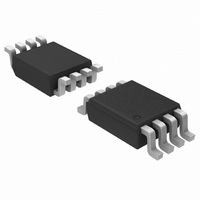
IC GATE OR DUAL LOGIC 2INP 8US8

NL27WZ32USG

Manufacturer Part Number
NL27WZ32USG
Description
IC GATE OR DUAL LOGIC 2INP 8US8
Manufacturer
ON Semiconductor
Series
7WZr
Datasheet

Specifications of NL27WZ32USG

Logic Type
OR Gate
Number Of Inputs
2
Number Of Circuits
2
Current - Output High, Low
32mA, 32mA
Voltage - Supply
1.65 V ~ 5.5 V
Operating Temperature
-40°C ~ 85°C
Mounting Type
Surface Mount
Package / Case
US8, 8-VSSOP
Lead Free Status / RoHS Status
Lead free / RoHS Compliant
Other names
NL27WZ32USGOS
NL27WZ32USGOS
NL27WZ32USGOSTR

Available stocks

Company
Part Number
Manufacturer
Quantity
Price
Part Number:
NL27WZ32USG
Manufacturer:
ON
Quantity:
18 000
Part Number:
NL27WZ32USG
Manufacturer:
ONSemicon
Quantity:
1 160
Part Number:
NL27WZ32USG
Manufacturer:
ON
Quantity:
8 000
Part Number:
NL27WZ32USG
Manufacturer:
ON/安森美
Quantity:
20 000
NL27WZ32
Dual 2−Input OR Gate
operating from a 1.65 V to 5.5 V supply.
Features
© Semiconductor Components Industries, LLC, 2006
April, 2006 − Rev. 6
GND
The NL27WZ32 is a high performance dual 2−input OR Gate
V
Power Requirements
Extremely High Speed: t
Designed for 1.65 V to 5.5 V V
Over Voltage Tolerant Inputs
LVTTL Compatible − Interface Capability With 5 V TTL Logic with
LVCMOS Compatible
24 mA Balanced Output Sink and Source Capability
Near Zero Static Supply Current Substantially Reduces System
Replacement for NC7WZ32
Chip Complexity: FET = 120
Pb−Free Package is Available
A1
B1
Y2
CC
= 3 V
1
2
3
4
PIN ASSIGNMENT
Pin
Figure 1. Pinout
1
2
3
4
5
6
7
8
Function
GND
V
A1
B1
Y2
A2
B2
Y1
CC
PD
2.5 ns (typical) at V
8
7
6
5
CC
V
Y1
B2
A2
CC
Operation
CC
= 5 V
1
*Date Code orientation may vary depending upon
See detailed ordering and shipping information in the
package dimensions section on page 4 of this data sheet.
manufacturing location.
(Note: Microdot may be in either location)
US SUFFIX
8
CASE 493
A1
B1
A2
B2
A
H
H
L
L
US8
ORDERING INFORMATION
LR
M
G
Figure 2. Logic Symbol
FUNCTION TABLE
Input
http://onsemi.com
1
= Device Code
= Date Code*
= Pb−Free Package
IEEE/IEC
w1
B
H
H
L
L
Publication Order Number:
MARKING
DIAGRAM
Y = A + B
Output
8
1
NL27WZ32/D
L4 M G
Y
H
H
H
L
Y1
Y2
G

Related parts for NL27WZ32USG

NL27WZ32USG Summary of contents

Page 1

NL27WZ32 Dual 2−Input OR Gate The NL27WZ32 is a high performance dual 2−input OR Gate operating from a 1. 5.5 V supply. Features • Extremely High Speed: t 2.5 ns (typical • Designed for 1.65 ...

Page 2

MAXIMUM RATINGS Symbol V DC Supply Voltage Input Voltage Output Voltage Input Diode Current Output Diode Current Output Sink Current Supply Current ...

Page 3

DC ELECTRICAL CHARACTERISTICS Symbol Parameter V HIGH Level Input Voltage IH V LOW Level Input Voltage IL V HIGH Level Output Voltage Low−Level Output Voltage Input ...

Page 4

... PHL PLH OUTPUT Y 50% 50% Figure 3. Switching Waveform DEVICE ORDERING INFORMATION Device Order Number NL27WZ32US NL27WZ32USG †For information on tape and reel specifications, including part orientation and tape sizes, please refer to our Tape and Reel Packaging Specifications Brochure, BRD8011/D. NL27WZ32 INPUT GND ...

Page 5

... ON Semiconductor Soldering and Mounting Techniques Reference Manual, SOLDERRM/D. N. American Technical Support: 800−282−9855 Toll Free USA/Canada Japan: ON Semiconductor, Japan Customer Focus Center 2−9−1 Kamimeguro, Meguro−ku, Tokyo, Japan 153−0051 Phone: 81−3−5773−3850 http://onsemi.com 5 NOTES: 1 ...

Related keywords