NL27WZ00USG ON Semiconductor, NL27WZ00USG Datasheet - Page 3
NL27WZ00USG
Manufacturer Part Number
NL27WZ00USG
Description
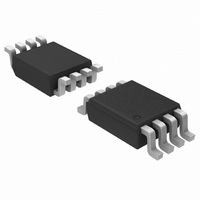
IC GATE NAND DUAL 2INPUT US8
Manufacturer
ON Semiconductor
Series
7WZr
Datasheet
1.NL27WZ00USG.pdf
(6 pages)
Specifications of NL27WZ00USG
Logic Type
NAND Gate
Number Of Inputs
2
Number Of Circuits
2
Current - Output High, Low
32mA, 32mA
Voltage - Supply
1.65 V ~ 5.5 V
Operating Temperature
-40°C ~ 85°C
Mounting Type
Surface Mount
Package / Case
US8, 8-VSSOP
Product
NAND
Logic Family
NL27WZ
High Level Output Current
- 32 mA
Low Level Output Current
32 mA
Propagation Delay Time
4.6 ns
Supply Voltage (max)
5.5 V
Supply Voltage (min)
1.65 V
Maximum Operating Temperature
+ 85 C
Mounting Style
SMD/SMT
Minimum Operating Temperature
- 40 C
Lead Free Status / RoHS Status
Lead free / RoHS Compliant
Other names
NL27WZ00USGOS
NL27WZ00USGOS
NL27WZ00USGOSTR
NL27WZ00USGOS
NL27WZ00USGOSTR
Available stocks
Company
Part Number
Manufacturer
Quantity
Price
Company:

Part Number:
NL27WZ00USG
Manufacturer:
ON
Quantity:
6 000
Company:
Part Number:
NL27WZ00USG
Manufacturer:
ON Semiconductor
Quantity:
8 650
Part Number:
NL27WZ00USG
Manufacturer:
ON/安森美
Quantity:
20 000


7. C
CAPACITIVE CHARACTERISTICS
DC ELECTRICAL CHARACTERISTICS
AC ELECTRICAL CHARACTERISTICS
High−Level Input
Voltage
Low−Level Input
Voltage
High−Level Output
Voltage
V
Low−Level Output
Voltage
V
Input Leakage
Current
Quiescent Supply
Current
Propagation Delay
(Figure 3 and 4)
Input Capacitance
Power Dissipation Capacitance
(Note 7)
IN
IN
Average operating current can be obtained by the equation: I
power consumption; P
PD
= V
= V
Parameter
Parameter
is defined as the value of the internal equivalent capacitance which is calculated from the operating current consumption without load.
IL
IH
or V
or V
IH
OH
Parameter
I
I
I
I
I
I
I
I
I
I
I
I
I
I
V
V
R
R
R
R
R
D
OH
OH
OH
OH
OH
OL
OL
OL
OL
OL
OH
OH
OL
OL
IN
IN
L
L
L
L
L
= C
= 1 MW, C
= 1 MW, C
= 500 W, C
= 1 MW, C
= 500 W, C
= 8 mA
= 12 mA
= 16 mA
= 24 mA
= 32 mA
= 100 mA
= 4 mA
= −8 mA
= −12 mA
= −16 mA
= −24 mA
= −32 mA
= −100 mA
= −4 mA
= V
= V
PD
Condition
Condition
CC
CC
V
or GND
or GND
CC
L
L
L
L
L
2
= 15 pF
= 15 pF
= 15 pF
= 50 pF
= 50 pF
f
in
+ I
t
R
CC
= t
V
Symbol
Symbol
F
V
10 MHz, V
10 MHz, V
V
= 3.0 ns
CC
V
t
t
V
I
V
PLH
PHL
I
CC
CC
OH
OL
IN
IH
IL
= 5.5 V, V
.
http://onsemi.com
CC(OPR
1.8 $ 0.15
1.65 to 5.5
1.65 to 5.5
CC
CC
2.5 $ 0.2
3.3 $ 0.3
5.0 $ 0.5
2.3 to 5.5
2.3 to 5.5
0 to 5.5
1.65
1.65
1.65
1.65
V
V
= 3.3 V, V
= 5.5 V, V
(V)
2.3
2.7
3.0
3.0
4.5
2.3
2.7
3.0
3.0
4.5
5.5
(V)
I
CC
CC
= 0 V or V
Condition
3
)
= C
PD
I
I
V
0.75 V
V
= 0 V or V
= 0 V or V
0.7 V
CC
CC
1.29
Min
Min
1.9
2.2
2.4
2.3
3.8
2.0
1.2
0.8
1.2
0.5
0.8
CC
− 0.1
CC
f
CC
in
T
T
A
A
CC
CC
+ I
= 255C
= 255C
0.08
0.20
0.22
0.28
0.38
0.42
CC
Typ
V
Typ
1.5
2.1
2.4
2.7
2.5
4.0
0.0
5.7
3.2
2.4
3.0
1.9
2.4
CC
. C
PD
0.25 V
0.3 V
Symbol
is used to determine the no−load dynamic
$0.1
Max
0.24
0.55
0.55
Max
10.5
C
0.1
0.3
0.4
0.4
1.0
5.3
3.7
4.6
2.9
3.6
C
PD
IN
CC
CC
−555C v T
−555C v T
V
0.75 V
0.7 V
CC
Min
1.29
Min
1.9
2.2
2.4
2.3
3.8
2.0
1.2
0.8
1.2
0.5
0.8
− 0.1
CC
CC
Typical
2.5
11
9
A
A
v 1255C
v 1255C
0.3 V
$1.0
Max
0.25
0.24
0.55
0.55
Max
11.0
0.1
0.3
0.4
0.4
5.7
4.0
4.9
3.2
3.9
10
CC
Unit
Unit
Unit
mA
mA
pF
pF
ns
V
V
V
V
Related parts for NL27WZ00USG
Image
Part Number
Description
Manufacturer
Datasheet
Request
R

Part Number:
Description:
ON Semiconductor [VOLTAGE REGULATOR]
Manufacturer:
ON Semiconductor
Datasheet:
Part Number:
Description:
357-036-542-201 CARDEDGE 36POS DL .156 BLK LOPRO
Manufacturer:
ON Semiconductor
Datasheet:
Part Number:
Description:
357-036-542-201 CARDEDGE 36POS DL .156 BLK LOPRO
Manufacturer:
ON Semiconductor
Datasheet:
Part Number:
Description:
357-036-542-201 CARDEDGE 36POS DL .156 BLK LOPRO
Manufacturer:
ON Semiconductor
Datasheet:
Part Number:
Description:
357-036-542-201 CARDEDGE 36POS DL .156 BLK LOPRO
Manufacturer:
ON Semiconductor
Datasheet:
Part Number:
Description:
357-036-542-201 CARDEDGE 36POS DL .156 BLK LOPRO
Manufacturer:
ON Semiconductor
Datasheet:
Part Number:
Description:
357-036-542-201 CARDEDGE 36POS DL .156 BLK LOPRO
Manufacturer:
ON Semiconductor
Datasheet:
Part Number:
Description:
357-036-542-201 CARDEDGE 36POS DL .156 BLK LOPRO
Manufacturer:
ON Semiconductor
Datasheet:
Part Number:
Description:
357-036-542-201 CARDEDGE 36POS DL .156 BLK LOPRO
Manufacturer:
ON Semiconductor
Datasheet:
Part Number:
Description:
357-036-542-201 CARDEDGE 36POS DL .156 BLK LOPRO
Manufacturer:
ON Semiconductor
Datasheet:
Part Number:
Description:
357-036-542-201 CARDEDGE 36POS DL .156 BLK LOPRO
Manufacturer:
ON Semiconductor
Datasheet:
Part Number:
Description:
Manufacturer:
ON Semiconductor
Datasheet:
Part Number:
Description:
Manufacturer:
ON Semiconductor
Datasheet:
Part Number:
Description:
Manufacturer:
ON Semiconductor
Datasheet: