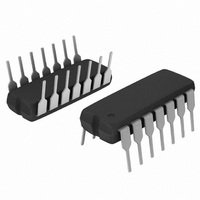
MC14001BCPG ON Semiconductor, MC14001BCPG Datasheet - Page 7

MC14001BCPG
Manufacturer Part Number
MC14001BCPG
Description
IC GATE NOR QUAD CMOS 14DIP
Manufacturer
ON Semiconductor
Series
4000Br
Specifications of MC14001BCPG
Logic Type
NOR Gate
Number Of Inputs
2
Number Of Circuits
4
Current - Output High, Low
3.4mA, 3.4mA
Voltage - Supply
3 V ~ 18 V
Operating Temperature
-55°C ~ 125°C
Mounting Type
Through Hole
Package / Case
14-DIP (0.300", 7.62mm)
Product
NOR
Logic Family
MC140
High Level Output Current
- 4.2 mA
Low Level Output Current
4.2 mA
Propagation Delay Time
250 ns
Supply Voltage (max)
18 V
Supply Voltage (min)
3 V
Maximum Operating Temperature
+ 125 C
Mounting Style
Through Hole
Minimum Operating Temperature
- 55 C
Circuit Type
Low-Power Schottky
Current, Supply
30 μA
Function Type
2-Inputs
Logic Function
NOR Gate
Package Type
PDIP-14
Temperature, Operating, Range
-55 to +125 °C
Voltage, Supply
3 to 18 VDC
Output Current
8.8mA
No. Of Inputs
2
Supply Voltage Range
3V To 18V
Logic Case Style
DIP
No. Of Pins
14
Operating Temperature Range
-55°C To +125°C
Filter Terminals
DIP
Rohs Compliant
Yes
Family Type
4000 CMOS
Lead Free Status / RoHS Status
Lead free / RoHS Compliant
Other names
MC14001BCPGOS
Available stocks
Company
Part Number
Manufacturer
Quantity
Price
Company:
Part Number:
MC14001BCPG
Manufacturer:
ON
Quantity:
1 000
Part Number:
MC14001BCPG
Manufacturer:
ON/安森美
Quantity:
20 000
5.0
4.0
3.0
2.0
1.0
8.0
6.0
4.0
2.0
16
14
12
10
0
0
0
0
1.0
2.0
Figure 10. V
2.0
4.0
Figure 8. V
V
V
V
V
O
O
out
V
in
in
, INPUT VOLTAGE (Vdc)
3.0
, INPUT VOLTAGE (Vdc)
6.0
0
SINGLE INPUT NAND, AND
MULTIPLE INPUT NOR, OR
(a) Inverting Function
V
TYPICAL B−SERIES GATE CHARACTERISTICS (cont’d)
SINGLE INPUT NOR, OR
MULTIPLE INPUT NAND, AND
DD
DD
4.0
DD
8.0
= 15 Vdc
V
= 5.0 Vdc
IL
SINGLE INPUT NOR, OR
MULTIPLE INPUT NAND, AND
SINGLE INPUT NAND, AND
MULTIPLE INPUT NOR, OR
5.0
10
VOLTAGE TRANSFER CHARACTERISTICS
V
Figure 11. DC Noise Immunity
IH
http://onsemi.com
V
V
DD
in
V
SS
= 0 VOLTS DC
7
from an ideal “1” or “0” input level which does not produce
output state change(s). The typical and guaranteed limit
values of the input values V
be at a fixed voltage V
Characteristics table. V
in Figure 11.
“0” levels =
The DC noise margin is defined as the input voltage range
Guaranteed minimum noise margins for both the “1” and
V
V
V
O
O
out
8.0
6.0
4.0
2.0
10
0
(b) Non−Inverting Function
0
0
1.0 V with a 5.0 V supply
2.0 V with a 10.0 V supply
2.5 V with a 15.0 V supply
V
DD
2.0
V
IL
4.0
DC NOISE MARGIN
Figure 9. V
V
IL
in
, INPUT VOLTAGE (Vdc)
6.0
and V
V
O
IH
SINGLE INPUT NAND, AND
MULTIPLE INPUT NOR, OR
IL
are given in the Electrical
SINGLE INPUT NOR, OR
MULTIPLE INPUT NAND, AND
and V
IH
8.0
DD
V
V
are presented graphically
DD
in
= 10 Vdc
IH
10
for the output(s) to


