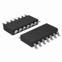
MC74ACT04DG ON Semiconductor, MC74ACT04DG Datasheet

MC74ACT04DG
Specifications of MC74ACT04DG
MC74ACT04DGOS
Related parts for MC74ACT04DG
MC74ACT04DG Summary of contents
Page 1
MC74AC04, MC74ACT04 Hex Inverter Features • Outputs Source/Sink 24 mA • ′ACT04 Has TTL Compatible Inputs • Pb−Free Packages are Available Figure 1. Pinout: 14−Lead Packages Conductors (Top ...
Page 2
RECOMMENDED OPERATING CONDITIONS Symbol V Supply Voltage Input Voltage, Output Voltage (Ref. to GND) in out Input Rise and Fall Time (Note ′AC Devices except Schmitt Inputs Input Rise ...
Page 3
... AC CHARACTERISTICS (For Figures and Waveforms − See Section 3 of the ON Semiconductor FACT Data Book, DL138/D) Symbol Parameter t Propagation Delay PLH t Propagation Delay PHL *Voltage Range 3 3.3 V ±0.3 V. Voltage Range 5 5.0 V ±0 CHARACTERISTICS Symbol Parameter V Minimum High Level IH Input Voltage V Maximum Low Level ...
Page 4
... AC CHARACTERISTICS (For Figures and Waveforms − See Section 3 of the ON Semiconductor FACT Data Book, DL138/D) Symbol Parameter t Propagation Delay PLH t Propagation Delay PHL *Voltage Range 5 5.0 V ±0.5 V. CAPACITANCE Symbol Parameter C Input Capacitance IN C Power Dissipation Capacitance PD 74ACT T = +25° (V) L Min ...
Page 5
... DEVICE ORDERING INFORMATION Device MC74AC04N MC74AC04NG MC74ACT04N MC74ACT04NG MC74AC04D MC74AC04DG MC74AC04DR2 MC74AC04DR2G MC74ACT04D MC74ACT04DG MC74ACT04DR2 MC74ACT04DR2G MC74AC04DT MC74AC04DTR2 MC74AC04DTR2G MC74ACT04DT MC74ACT04DTR2 MC74ACT04DTR2G MC74AC04MEL MC74AC04MELG MC74ACT04M MC74ACT04MG MC74ACT04MEL MC74ACT04MELG †For information on tape and reel specifications, including part orientation and tape sizes, please refer to our Tape and Reel Packaging Specifications Brochure, BRD8011/D. *This package is inherently Pb− ...
Page 6
PDIP− MC74AC04N AWLYYWWG MC74ACT04N AWLYYWWG 1 1 MARKING DIAGRAMS SOIC−14 TSSOP− AC04G 04 AWLYWW ALYWG ACT ACT04G 04 AWLYWW ALYWG Assembly Location WL ...
Page 7
−T− SEATING PLANE 0.13 (0.005) PACKAGE DIMENSIONS PDIP−14 CASE 646−06 ISSUE http://onsemi.com 7 NOTES: 1. DIMENSIONING AND TOLERANCING PER ANSI ...
Page 8
... G −T− SEATING 14 PL PLANE 0.25 (0.010 14X 0.58 *For additional information on our Pb−Free strategy and soldering details, please download the ON Semiconductor Soldering and Mounting Techniques Reference Manual, SOLDERRM/D. PACKAGE DIMENSIONS SOIC−14 CASE 751A−03 ISSUE 0.25 (0.010 ...
Page 9
... S A −V− C 0.10 (0.004) −T− SEATING G D PLANE 14X 0.36 *For additional information on our Pb−Free strategy and soldering details, please download the ON Semiconductor Soldering and Mounting Techniques Reference Manual, SOLDERRM/D. PACKAGE DIMENSIONS TSSOP−14 CASE 948G−01 ISSUE 0.25 (0.010) ...
Page 10
... Opportunity/Affirmative Action Employer. This literature is subject to all applicable copyright laws and is not for resale in any manner. PUBLICATION ORDERING INFORMATION LITERATURE FULFILLMENT: Literature Distribution Center for ON Semiconductor P.O. Box 5163, Denver, Colorado 80217 USA Phone: 303−675−2175 or 800−344−3860 Toll Free USA/Canada Fax: 303− ...


