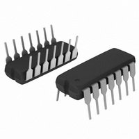
MC74AC08NG ON Semiconductor, MC74AC08NG Datasheet

MC74AC08NG
Specifications of MC74AC08NG
Related parts for MC74AC08NG
MC74AC08NG Summary of contents
Page 1
MC74AC08, MC74ACT08 Quad 2-Input AND Gate Features • Outputs Source/Sink 24 mA • ′ACT08 Has TTL Compatible Inputs • Pb−Free Packages are Available MAXIMUM RATINGS Rating DC Supply Voltage (Referenced to GND) DC Input Voltage (Referenced to GND) DC Output ...
Page 2
RECOMMENDED OPERATING CONDITIONS Symbol V Supply Voltage Input Voltage, Output Voltage (Ref. to GND) in out Input Rise and Fall Time (Note ′AC Devices except Schmitt Inputs Input Rise ...
Page 3
... AC CHARACTERISTICS (For Figures and Waveforms − See Section 3 of the ON Semiconductor FACT Data Book, DL138/D) Symbol Parameter t Propagation Delay PLH t Propagation Delay PHL 5. Voltage Range 3 3.3 V ±0.3 V. Voltage Range 5 5.0 V ±0 CHARACTERISTICS Symbol Parameter V Minimum High Level IH Input Voltage V Maximum Low Level ...
Page 4
... AC CHARACTERISTICS (For Figures and Waveforms − See Section 3 of the ON Semiconductor FACT Data Book, DL138/D) Symbol Parameter t Propagation Delay PLH t Propagation Delay PHL 8. Voltage Range 5 5.0 V ±0.5 V. CAPACITANCE Symbol Parameter C Input Capacitance IN C Power Dissipation Capacitance PD 74ACT T = +25° (V) CC Min ...
Page 5
... PDIP− MC74AC08N AWLYYWWG MC74ACT08N AWLYYWWG 1 ORDERING INFORMATION Device MC74AC08NG MC74AC08D MC74AC08DG MC74AC08DR2 MC74AC08DR2G MC74AC08DTR2 MC74AC08DTR2G MC74AC08MEL MC74AC08MELG MC74ACT08N MC74ACT08NG MC74ACT08D MC74ACT08DG MC74ACT08DR2 MC74ACT08DR2G MC74ACT08DR2GH (Pb−Free, Halide−Free) MC74ACT08DTR2 MC74ACT08DTR2G MC74ACT08MELG †For information on tape and reel specifications, including part orientation and tape sizes, please refer to our Tape and Reel Packaging Specifications Brochure, BRD8011/D. *This package is inherently Pb− ...
Page 6
−T− SEATING PLANE 0.13 (0.005) PACKAGE DIMENSIONS PDIP−14 CASE 646−06 ISSUE http://onsemi.com 6 NOTES: 1. DIMENSIONING AND TOLERANCING PER ANSI ...
Page 7
... G −T− SEATING 14 PL PLANE 0.25 (0.010 14X 0.58 *For additional information on our Pb−Free strategy and soldering details, please download the ON Semiconductor Soldering and Mounting Techniques Reference Manual, SOLDERRM/D. PACKAGE DIMENSIONS SOIC−14 CASE 751A−03 ISSUE 0.25 (0.010 ...
Page 8
... S A −V− C 0.10 (0.004) −T− G SEATING D PLANE 14X 0.36 *For additional information on our Pb−Free strategy and soldering details, please download the ON Semiconductor Soldering and Mounting Techniques Reference Manual, SOLDERRM/D. PACKAGE DIMENSIONS TSSOP−14 CASE 948G−01 ISSUE 0.25 (0.010) ...
Page 9
... Opportunity/Affirmative Action Employer. This literature is subject to all applicable copyright laws and is not for resale in any manner. PUBLICATION ORDERING INFORMATION LITERATURE FULFILLMENT: Literature Distribution Center for ON Semiconductor P.O. Box 5163, Denver, Colorado 80217 USA Phone: 303−675−2175 or 800−344−3860 Toll Free USA/Canada Fax: 303− ...


