M74VHC1G132DFT2G ON Semiconductor, M74VHC1G132DFT2G Datasheet - Page 3
M74VHC1G132DFT2G
Manufacturer Part Number
M74VHC1G132DFT2G
Description
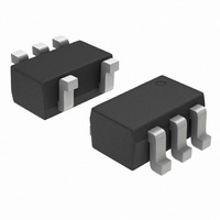
IC GATE NAND SGL SCHMITT SOT-353
Manufacturer
ON Semiconductor
Series
74VHCr
Datasheet
1.M74VHC1G132DFT1G.pdf
(6 pages)
Specifications of M74VHC1G132DFT2G
Logic Type
NAND Gate - Schmitt Trigger
Number Of Inputs
2
Number Of Circuits
1
Current - Output High, Low
8mA, 8mA
Voltage - Supply
2 V ~ 5.5 V
Operating Temperature
-55°C ~ 125°C
Mounting Type
Surface Mount
Package / Case
SC-70-5, SC-88A, SOT-323-5, SOT-353, 5-TSSOP
Lead Free Status / RoHS Status
Lead free / RoHS Compliant
Available stocks
Company
Part Number
Manufacturer
Quantity
Price
Company:

Part Number:
M74VHC1G132DFT2G
Manufacturer:
ON Semiconductor
Quantity:
4 750


Î Î Î Î Î Î Î Î Î Î Î Î Î Î Î Î Î Î Î Î Î Î Î Î Î Î Î Î Î Î Î Î Î
Î Î Î Î
Î Î Î Î
Î Î Î Î
Î Î Î Î
Î Î Î Î
Î Î Î Î
Î Î Î Î
Î Î Î Î
Î Î Î Î
Î Î Î Î
6. C
AC ELECTRICAL CHARACTERISTICS
DC ELECTRICAL CHARACTERISTICS
Symbol
Symbol
t
V
t
C
V
V
V
Average operating current can be obtained by the equation: I
power consumption; P
PLH
C
I
V
PHL
I
CC
OH
IN
T+
T−
OL
PD
PD
IN
H
,
is defined as the value of the internal equivalent capacitance which is calculated from the operating current consumption without load.
Î Î Î Î Î Î Î
Î Î Î Î Î Î Î
Î Î Î Î Î Î Î
Î Î Î Î Î Î Î
Î Î Î Î Î Î Î
Î Î Î Î Î Î Î
Î Î Î Î Î Î Î
Î Î Î Î Î Î Î
Î Î Î Î Î Î Î
Î Î Î Î Î Î Î
Positive Threshold
Voltage
Negative Threshold
Voltage
Hysteresis Voltage
Minimum High−Level
Output Voltage
I
Maximum Low−Level
Output Voltage
Maximum Input
Leakage Current
Maximum Quiescent
Supply Current
Maximum Propagation
Delay, A or B to Y
Maximum Input Capaci-
tance
Power Dissipation Capacitance (Note 6)
OH
= −50mA
Parameter
Parameter
D
= C
PD
V
CC
Î Î Î Î Î Î Î Î
Î Î Î Î Î Î Î Î
Î Î Î Î Î Î Î Î
Î Î Î Î Î Î Î Î
Î Î Î Î Î Î Î Î
Î Î Î Î Î Î Î Î
Î Î Î Î Î Î Î Î
Î Î Î Î Î Î Î Î
Î Î Î Î Î Î Î Î
Î Î Î Î Î Î Î Î
Î Î Î Î Î Î Î Î Î Î Î
2
V
V
I
I
I
V
I
I
I
V
V
V
V
OH
OH
OH
OL
OL
OL
f
IN
IN
IN
IN
IN
CC
CC
Test Conditions
in
= 50 mA
= 4 mA
= 8 mA
= V
= V
= −50 mA
= −4 mA
= −8 mA
= V
= 5.5 V or GND
= V
= 3.3 ± 0.3 V C
= 5.0 ± 0.5 V C
C
+ I
Test Conditions
load
CC
IH
IH
CC
CC
or V
or V
or GND
or GND
= 50 pF, Input t
V
IL
IL
CC
MC74VHC1G132
.
http://onsemi.com
C
C
L
L
L
L
CC(OPR
= 15 pF
= 50 pF
= 15 pF
= 50 pF
V
0 to
r
(V)
3.0
4.5
5.5
3.0
4.5
5.5
3.0
4.5
5.5
2.0
3.0
4.5
3.0
4.5
2.0
3.0
4.5
3.0
4.5
5.5
5.5
/t
CC
3
f
)
Î Î Î Î Î Î Î
Î Î Î Î Î Î Î
Î Î Î
Î Î Î
Î Î Î
Î Î Î
Î Î Î
Î Î Î
Î Î Î
Î Î Î
Î Î Î Î Î Î
= 3.0 ns
= C
PD
1.50
2.35
2.80
0.65
1.10
1.45
0.30
0.40
0.50
2.58
3.94
Min
Min
1.9
2.9
4.4
V
Î Î Î
Î Î Î
Î Î Î
Î Î Î
Î Î Î
Î Î Î
Î Î Î
Î Î Î
Î Î Î
T
T
CC
A
A
1.88
2.66
3.21
1.03
1.62
2.02
0.85
1.05
1.20
= 25°C
Typ
= 25°C
Typ
2.0
3.0
4.5
0.0
0.0
0.0
4.6
6.1
3.6
4.3
5.5
f
in
Î Î Î
Î Î Î
Î Î Î
Î Î Î
Î Î Î
Î Î Î
Î Î Î
Î Î Î
Î Î Î
Î Î Î
+ I
Typical @ 25°C, V
CC
Max
2.25
3.10
3.70
1.40
2.10
2.60
1.60
2.00
2.25
0.36
0.36
±0.1
Max
11.9
15.4
0.1
0.1
0.1
1.0
7.7
9.7
10
. C
PD
Î Î Î Î
Î Î Î Î
Î Î
Î Î
Î Î Î Î
Î Î
Î Î
Î Î Î Î
Î Î Î Î Î Î Î
1.50
2.35
2.80
0.65
1.10
1.45
0.30
0.40
0.50
2.48
3.80
Min
Min
1.9
2.9
4.4
1.0
1.0
1.0
1.0
is used to determine the no−load dynamic
T
T
A
A
Î Î Î
Î Î Î
Î Î Î
Î Î Î
Î Î Î
Î Î Î
Î Î Î
Î Î Î
Î Î Î
11
≤ 85°C
≤ 85°C
Max
2.25
3.10
3.70
1.40
2.10
2.60
1.60
2.00
2.25
0.44
0.44
±1.0
Max
14.0
17.5
11.0
0.1
0.1
0.1
9.0
20
10
CC
Î Î Î Î Î Î
Î Î Î Î Î Î
Î Î Î
Î Î Î
Î Î Î
Î Î Î
Î Î Î
Î Î Î
Î Î Î
Î Î Î
Î Î Î
Î Î Î Î Î Î Î
= 5.0 V
−55 ≤ T
−55 ≤ T
1.50
2.35
2.80
0.65
1.10
1.45
0.30
0.40
0.50
2.34
3.66
Min
Min
1.9
2.9
4.5
1.0
1.0
1.0
1.0
Î Î Î Î
Î Î Î Î
Î Î Î Î
Î Î Î Î
Î Î Î Î
Î Î Î Î
Î Î Î Î
Î Î Î Î
Î Î Î Î
A
A
≤ 125°C
≤ 125°C
Max
2.25
3.10
3.70
1.40
2.10
2.60
1.60
2.00
2.25
0.52
0.52
±1.0
Max
16.1
19.6
10.3
12.3
0.1
0.1
0.1
40
10
Î Î
Î Î Î Î
Î Î Î Î
Î Î
Î Î Î Î
Î Î Î Î
Unit
Unit
mA
mA
ns
pF
pF
V
V
V
V
V
V
V
Related parts for M74VHC1G132DFT2G
Image
Part Number
Description
Manufacturer
Datasheet
Request
R

Part Number:
Description:
ON Semiconductor [VOLTAGE REGULATOR]
Manufacturer:
ON Semiconductor
Datasheet:
Part Number:
Description:
357-036-542-201 CARDEDGE 36POS DL .156 BLK LOPRO
Manufacturer:
ON Semiconductor
Datasheet:
Part Number:
Description:
357-036-542-201 CARDEDGE 36POS DL .156 BLK LOPRO
Manufacturer:
ON Semiconductor
Datasheet:
Part Number:
Description:
357-036-542-201 CARDEDGE 36POS DL .156 BLK LOPRO
Manufacturer:
ON Semiconductor
Datasheet:
Part Number:
Description:
357-036-542-201 CARDEDGE 36POS DL .156 BLK LOPRO
Manufacturer:
ON Semiconductor
Datasheet:
Part Number:
Description:
357-036-542-201 CARDEDGE 36POS DL .156 BLK LOPRO
Manufacturer:
ON Semiconductor
Datasheet:
Part Number:
Description:
357-036-542-201 CARDEDGE 36POS DL .156 BLK LOPRO
Manufacturer:
ON Semiconductor
Datasheet:
Part Number:
Description:
357-036-542-201 CARDEDGE 36POS DL .156 BLK LOPRO
Manufacturer:
ON Semiconductor
Datasheet:
Part Number:
Description:
357-036-542-201 CARDEDGE 36POS DL .156 BLK LOPRO
Manufacturer:
ON Semiconductor
Datasheet:
Part Number:
Description:
357-036-542-201 CARDEDGE 36POS DL .156 BLK LOPRO
Manufacturer:
ON Semiconductor
Datasheet:
Part Number:
Description:
357-036-542-201 CARDEDGE 36POS DL .156 BLK LOPRO
Manufacturer:
ON Semiconductor
Datasheet:
Part Number:
Description:
Manufacturer:
ON Semiconductor
Datasheet:
Part Number:
Description:
Manufacturer:
ON Semiconductor
Datasheet:
Part Number:
Description:
Manufacturer:
ON Semiconductor
Datasheet: