MC14106BDTR2G ON Semiconductor, MC14106BDTR2G Datasheet
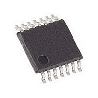
IC SCHMITT TRIGGER HEX 14-TSSOP

MC14106BDTR2G

Manufacturer Part Number
MC14106BDTR2G
Description
IC SCHMITT TRIGGER HEX 14-TSSOP
Manufacturer
ON Semiconductor
Series
4000Br
Datasheet

Specifications of MC14106BDTR2G

Logic Type
Inverter with Schmitt Trigger
Number Of Inputs
1
Number Of Circuits
6
Current - Output High, Low
3.4mA, 3.4mA
Voltage - Supply
3 V ~ 18 V
Operating Temperature
-55°C ~ 125°C
Mounting Type
Surface Mount
Package / Case
14-TSSOP
Logical Function
Inverter Schmit Trig
Logic Family
4000
Number Of Elements
6
Input Type
Schmitt Trigger
High Level Output Current
-4.2mA
Low Level Output Current
4.2mA
Propagation Delay Time
250ns
Operating Supply Voltage (typ)
3.3/5/9/12/15V
Package Type
TSSOP
Operating Temp Range
-55C to 125C
Pin Count
14
Quiescent Current
1uA
Output Type
Schmitt Trigger
Technology
CMOS
Mounting
Surface Mount
Operating Temperature Classification
Military
Operating Supply Voltage (max)
18V
Operating Supply Voltage (min)
3V
Lead Free Status / RoHS Status
Lead free / RoHS Compliant

Available stocks

Company
Part Number
Manufacturer
Quantity
Price
Part Number:
MC14106BDTR2G
Manufacturer:
ON
Quantity:
5 510
Part Number:
MC14106BDTR2G
Manufacturer:
ON Semiconductor
Quantity:
1 900
MC14106B
Hex Schmitt Trigger
P−channel and N−channel enhancement mode devices in a single
monolithic structure. These devices find primary use where low power
dissipation and/or high noise immunity is desired. The MC14106B
may be used in place of the MC14069UB hex inverter for enhanced
noise immunity or to “square up” slowly changing waveforms.
due to high static voltages or electric fields. However, precautions
must be taken to avoid applications of any voltage higher than
maximum rated voltages to this high−impedance circuit. For proper
operation, V
or V
level (e.g., either V
Features
Stresses exceeding Maximum Ratings may damage the device. Maximum
Ratings are stress ratings only. Functional operation above the Recommended
Operating Conditions is not implied. Extended exposure to stresses above the
Recommended Operating Conditions may affect device reliability.
1. Temperature Derating: Plastic “P and D/DW” Packages: – 7.0 mW/°C From
MAXIMUM RATINGS
© Semiconductor Components Industries, LLC, 2006
October, 2006 − Rev. 7
Symbol
V
I
The MC14106B hex Schmitt Trigger is constructed with MOS
This device contains protection circuitry to guard against damage
Unused inputs must always be tied to an appropriate logic voltage
in
Schottky TTL Load Over the Rated Temperature Range
in
Increased Hysteresis Voltage Over the MC14584B
Supply Voltage Range = 3.0 Vdc to 18 Vdc
Capable of Driving Two Low−power TTL Loads or One Low−power
Pin−for−Pin Replacement for CD40106B and MM74C14
Can Be Used to Replace the MC14584B or MC14069UB
Pb−Free Packages are Available
V
T
65°C To 125°C
P
, V
, I
T
T
stg
out
DD
A
D
L
out
out
) v V
DC Supply Voltage Range
Input or Output Voltage Range
Input or Output Current
Power Dissipation, per Package
Ambient Temperature Range
Storage Temperature Range
Lead Temperature
in
DD
(DC or Transient)
(DC or Transient) per Pin
(Note 1)
(8−Second Soldering)
and V
.
SS
out
Parameter
or V
(Voltages Referenced to V
should be constrained to the range V
DD
). Unused outputs must be left open.
−0.5 to V
SS
−0.5 to +18.0
−55 to +125
−65 to +150
)
Value
± 10
500
260
DD
+ 0.5
SS
1
v (V
Unit
mW
mA
°C
°C
°C
V
V
in
See detailed ordering and shipping information in the package
dimensions section on page 2 of this data sheet.
14
(Note: Microdot may be in either location)
CASE 948G
CASE 751A
DT SUFFIX
TSSOP−14
CASE 646
P SUFFIX
D SUFFIX
PDIP−14
SOIC−14
ORDERING INFORMATION
A
WL, L
YY, Y
WW, W = Work Week
G or G
http://onsemi.com
1
= Assembly Location
= Wafer Lot
= Year
= Pb−Free Package
Publication Order Number:
14
1
14
1
14
MC14106BCP
DIAGRAMS
AWLYYWWG
1
MARKING
AWLYWW
MC14106B/D
14106BG
ALYWG
106B
14
G

Related parts for MC14106BDTR2G

MC14106BDTR2G Summary of contents

Page 1

MC14106B Hex Schmitt Trigger The MC14106B hex Schmitt Trigger is constructed with MOS P−channel and N−channel enhancement mode devices in a single monolithic structure. These devices find primary use where low power dissipation and/or high noise immunity is desired. The ...

Page 2

... MC14106BCPG MC14106BD MC14106BDG MC14106BDR2 MC14106BDR2G MC14106BDTR2 MC14106BDTR2G †For information on tape and reel specifications, including part orientation and tape sizes, please refer to our Tape and Reel Packaging Specifications Brochure, BRD8011/D. *This package is inherently Pb−Free. Figure 2. Equivalent Circuit Schematic (1/6 of Circuit Shown) Package PDIP− ...

Page 3

ELECTRICAL CHARACTERISTICS Î Î Î Î Î ...

Page 4

SWITCHING CHARACTERISTICS Î Î Î Î Î ...

Page 5

out (a) Schmitt Triggers will square up inputs with slow rise and fall times Useful as Pushbutton/Keyboard Debounce Circuit. APPLICATIONS V V out ...

Page 6

– – – – – – ...

Page 7

−T− SEATING PLANE 0.13 (0.005) PACKAGE DIMENSIONS PDIP−14 CASE 646−06 ISSUE http://onsemi.com 7 NOTES: 1. DIMENSIONING AND TOLERANCING PER ANSI ...

Page 8

... G −T− SEATING 14 PL PLANE 0.25 (0.010 14X 0.58 *For additional information on our Pb−Free strategy and soldering details, please download the ON Semiconductor Soldering and Mounting Techniques Reference Manual, SOLDERRM/D. PACKAGE DIMENSIONS SOIC−14 CASE 751A−03 ISSUE 0.25 (0.010 ...

Page 9

... S A −V− C 0.10 (0.004) −T− SEATING G D PLANE 14X 0.36 *For additional information on our Pb−Free strategy and soldering details, please download the ON Semiconductor Soldering and Mounting Techniques Reference Manual, SOLDERRM/D. PACKAGE DIMENSIONS TSSOP−14 CASE 948G−01 ISSUE 0.25 (0.010) ...

Page 10

... Opportunity/Affirmative Action Employer. This literature is subject to all applicable copyright laws and is not for resale in any manner. PUBLICATION ORDERING INFORMATION LITERATURE FULFILLMENT: Literature Distribution Center for ON Semiconductor P.O. Box 5163, Denver, Colorado 80217 USA Phone: 303−675−2175 or 800−344−3860 Toll Free USA/Canada Fax: 303− ...

Related keywords