MC74ACT14DG ON Semiconductor, MC74ACT14DG Datasheet
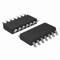
IC SCHMITT TRIG HEX INV 14-SOIC

MC74ACT14DG

Manufacturer Part Number
MC74ACT14DG
Description
IC SCHMITT TRIG HEX INV 14-SOIC
Manufacturer
ON Semiconductor
Series
74ACTr
Datasheet

Specifications of MC74ACT14DG

Logic Type
Inverter with Schmitt Trigger
Number Of Inputs
1
Number Of Circuits
6
Current - Output High, Low
24mA, 24mA
Voltage - Supply
4.5 V ~ 5.5 V
Operating Temperature
-40°C ~ 85°C
Mounting Type
Surface Mount
Package / Case
14-SOIC (3.9mm Width), 14-SOL
Logic Family
74ACT
High Level Output Current
- 24 mA
Low Level Output Current
24 mA
Supply Voltage (max)
5.5 V
Supply Voltage (min)
4.5 V
Maximum Operating Temperature
+ 85 C
Mounting Style
SMD/SMT
Operating Supply Voltage
2 V to 6 V
Logical Function
Inverter Schmit Trig
Number Of Elements
6
Input Type
Schmitt Trigger
Propagation Delay Time
15ns
Operating Supply Voltage (typ)
5V
Package Type
SOIC
Operating Temp Range
-40C to 85C
Pin Count
14
Quiescent Current
4uA
Output Type
Schmitt Trigger
Technology
CMOS
Mounting
Surface Mount
Operating Temperature Classification
Industrial
Operating Supply Voltage (max)
5.5V
Operating Supply Voltage (min)
4.5V
Lead Free Status / RoHS Status
Lead free / RoHS Compliant
Other names
MC74ACT14DG
MC74ACT14DGOS
MC74AC14, MC74ACT14
Hex Inverter Schmitt
Trigger
accept standard CMOS Input signals (TTL levels for MC74ACT14)
and provide standard CMOS output levels. They are capable of
transforming slowly changing input signals into sharply defined,
jitter−free output signals. In addition, they have a greater noise margin
then conventional inverters.
positive−going and negative−going input thresholds (typically 1.0 V)
which is determined internally by transistor ratios and is essentially
insensitive to temperature and supply voltage variations.
Features
Stresses exceeding Maximum Ratings may damage the device. Maximum
Ratings are stress ratings only. Functional operation above the Recommended
Operating Conditions is not implied. Extended exposure to stresses above the
Recommended Operating Conditions may affect device reliability.
MAXIMUM RATINGS
© Semiconductor Components Industries, LLC, 2006
October, 2006 − Rev. 7
DC Supply Voltage (Referenced to GND)
DC Input Voltage (Referenced to GND)
DC Output Voltage (Referenced to GND)
DC Input Current, per Pin
DC Output Sink/Source Current, per Pin
DC V
Storage Temperature
The MC74AC14/74ACT14 contains six logic inverters which
The MC74AC14/74ACT14 has hysteresis between the
Schmitt Trigger Inputs
Outputs Source/Sink 24 mA
′ACT14 Has TTL Compatible Inputs
Pb−Free Packages are Available
CC
or GND Current per Output Pin
Rating
Symbol
V
V
T
I
I
V
I
CC
out
CC
out
stg
in
in
−0.5 to V
−0.5 to V
−0.5 to +7.0
−65 to +150
Value
±20
±50
±50
CC
CC
+0.5
+0.5
1
Unit
mA
mA
mJ
°C
V
V
V
See detailed ordering and shipping information in the package
dimensions section on page 4 of this data sheet.
See general marking information in the device marking
section on page 5 of this data sheet.
V
CC
14
Figure 1. Pinout: 14−Lead Packages
14
14
14
DEVICE MARKING INFORMATION
14
1
1
ORDERING INFORMATION
1
13
2
1
1
http://onsemi.com
FUNCTION TABLE
Input
A
H
L
12
Conductors
3
(Top View)
11
Publication Order Number:
4
Output
10
5
O
H
L
CASE 948G
CASE 751A
SOEIAJ−14
SUFFIX DT
TSSOP−14
CASE 646
SUFFIX M
CASE 965
SUFFIX N
SUFFIX D
PDIP−14
SOIC−14
MC74AC14/D
9
6
8
7
GND

Related parts for MC74ACT14DG

MC74ACT14DG Summary of contents

Page 1

MC74AC14, MC74ACT14 Hex Inverter Schmitt Trigger The MC74AC14/74ACT14 contains six logic inverters which accept standard CMOS Input signals (TTL levels for MC74ACT14) and provide standard CMOS output levels. They are capable of transforming slowly changing input signals into sharply defined, ...

Page 2

... NOTE: I and I @ 3.0 V are guaranteed to be less than or equal to the respective limit @ 5 CHARACTERISTICS (For Figures and Waveforms − See Section 3 of the ON Semiconductor FACT Data Book, DL138/D) Symbol Parameter t Propagation Delay PLH t Propagation Delay PHL *Voltage Range 3 3.3 V ± ...

Page 3

... Maximum Quiescent Supply Current CC *All outputs loaded; thresholds on input associated with output under test. †Maximum test duration 2.0 ms, one output loaded at a time. AC CHARACTERISTICS (For Figures and Waveforms − See Section 3 of the ON Semiconductor FACT Data Book, DL138/D) Symbol Parameter t Propagation Delay ...

Page 4

... ORDERING INFORMATION Device MC74AC14N MC74AC14NG MC74ACT14N MC74ACT14NG MC74AC14D MC74AC14DG MC74AC14DR2 MC74AC14DR2G MC74ACT14D MC74ACT14DG MC74ACT14DR2 MC74ACT14DR2G MC74AC14DTR2 MC74AC14DTR2G MC74ACT14DTR2 MC74ACT14DTR2G MC74AC14MEL MC74AC14MELG MC74ACT14MEL MC74ACT14MELG †For information on tape and reel specifications, including part orientation and tape sizes, please refer to our Tape and Reel Packaging Specifications Brochure, BRD8011/D. *This package is inherently Pb− ...

Page 5

PDIP− MC74AC14N AWLYYWWG MC74ACT14N AWLYYWWG 1 1 (Note: Microdot may be in either location) MARKING DIAGRAMS SOIC−14 TSSOP− AC14G 14 AWLYWW ALYWG ACT ACT14G 14 AWLYWW ALYWG G 1 ...

Page 6

−T− SEATING PLANE 0.13 (0.005) PACKAGE DIMENSIONS PDIP−14 CASE 646−06 ISSUE http://onsemi.com 6 NOTES: 1. DIMENSIONING AND TOLERANCING PER ANSI ...

Page 7

... G −T− SEATING 14 PL PLANE 0.25 (0.010 14X 0.58 *For additional information on our Pb−Free strategy and soldering details, please download the ON Semiconductor Soldering and Mounting Techniques Reference Manual, SOLDERRM/D. PACKAGE DIMENSIONS SOIC−14 CASE 751A−03 ISSUE 0.25 (0.010 ...

Page 8

... S A −V− C 0.10 (0.004) −T− SEATING G D PLANE 14X 0.36 *For additional information on our Pb−Free strategy and soldering details, please download the ON Semiconductor Soldering and Mounting Techniques Reference Manual, SOLDERRM/D. PACKAGE DIMENSIONS TSSOP−14 CASE 948G−01 ISSUE 0.25 (0.010) ...

Page 9

... Opportunity/Affirmative Action Employer. This literature is subject to all applicable copyright laws and is not for resale in any manner. PUBLICATION ORDERING INFORMATION LITERATURE FULFILLMENT: Literature Distribution Center for ON Semiconductor P.O. Box 5163, Denver, Colorado 80217 USA Phone: 303−675−2175 or 800−344−3860 Toll Free USA/Canada Fax: 303− ...

Related keywords