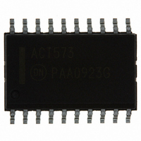
MC74ACT573DWG ON Semiconductor, MC74ACT573DWG Datasheet

MC74ACT573DWG
Specifications of MC74ACT573DWG
MC74ACT573DWGOS
Related parts for MC74ACT573DWG
MC74ACT573DWG Summary of contents
Page 1
... Output Enable Input O −O 3−State Latch Outputs Figure 2. Logic Symbol *For additional information on our Pb−Free strategy and soldering details, please download the ON Semiconductor Soldering and Mounting Techniques Reference Manual, SOLDERRM/D. © Semiconductor Components Industries, LLC, 2005 September, 2005 − Rev GND http://onsemi ...
Page 2
TRUTH TABLE Inputs HIGH Voltage Level L = LOW Voltage Level Z = High Impedance X = Immaterial O = Previous O ...
Page 3
MAXIMUM RATINGS Symbol V DC Supply Voltage (Referenced to GND Input Voltage (Referenced to GND Output Voltage (Referenced to GND) OUT I DC Input Current, per Pin Output Sink/Source Current, per ...
Page 4
DC CHARACTERISTICS Symbol Parameter V Minimum High Level IH Input Voltage V Maximum Low Level IL Input Voltage V Minimum High Level OH Output Voltage V Maximum Low Level OL Output Voltage I Maximum Input IN Leakage Current I Maximum ...
Page 5
AC CHARACTERISTICS (For Figures and Waveforms − See Section 3) Symbol Parameter Propagation Delay t PLH Propagation Delay t PHL Propagation Delay t PLH Propagation Delay ...
Page 6
DC CHARACTERISTICS Symbol Parameter V Minimum High Level IH Input Voltage V Maximum Low Level IL Input Voltage V Minimum High Level OH Output Voltage V Maximum Low Level OL Output Voltage I Maximum Input IN Leakage Current DI Additional ...
Page 7
AC OPERATING REQUIREMENTS Symbol Parameter Setup Time, HIGH or LOW Hold Time, HIGH or LOW Pulse Width, HIGH w *Voltage Range 5 5.0 V ...
Page 8
... MC74AC573DWR2 MC74AC573DWR2G MC74AC573DTR2 MC74AC573DTR2G MC74AC573MEL MC74AC573MELG MC74ACT573N MC74ACT573NG MC74ACT573DW MC74ACT573DWG MC74ACT573DWR2 MC74ACT573DWR2G MC74ACT573DTR2 MC74ACT573DTR2G †For information on tape and reel specifications,including part orientation and tape sizes, please refer to our Tape and Reel Packaging Specifications Brochure, BRD8011/D. *This package is inherently Pb−Free. MC74AC573, MC74ACT573 ...
Page 9
SEATING PLANE 0.25 (0.010 20X 0. 18X MC74AC573, MC74ACT573 PACKAGE DIMENSIONS PDIP−20 N SUFFIX 20 PIN ...
Page 10
MC74AC573, MC74ACT573 20 PIN PLASTIC TSSOP PACKAGE K 20X REF 0.10 (0.004) 0.15 (0.006 L PIN 1 IDENT 1 0.15 (0.006 −V− 0.100 (0.004) SEATING −T− PLANE ...
Page 11
0.13 (0.005) 0.10 (0.004) M MC74AC573, MC74ACT573 PACKAGE DIMENSIONS SOEIAJ−20 M SUFFIX 20 PIN PLASTIC EIAJ PACKAGE CASE 967−01 ISSUE DETAIL ...
Page 12
... Fax: 480−829−7709 or 800−344−3867 Toll Free USA/Canada Email: orderlit@onsemi.com MC74AC573, MC74ACT573 N. American Technical Support: 800−282−9855 Toll Free USA/Canada Japan: ON Semiconductor, Japan Customer Focus Center 2−9−1 Kamimeguro, Meguro−ku, Tokyo, Japan 153−0051 Phone: 81−3−5773−3850 http://onsemi.com 12 ON Semiconductor Website: http://onsemi ...


