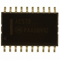
MC74AC573DWR2G ON Semiconductor, MC74AC573DWR2G Datasheet - Page 3

MC74AC573DWR2G
Manufacturer Part Number
MC74AC573DWR2G
Description
IC LATCH OCTAL 20-SOIC
Manufacturer
ON Semiconductor
Series
74ACr
Type
D-Typer
Datasheet
1.MC74ACT573DWG.pdf
(12 pages)
Specifications of MC74AC573DWR2G
Logic Type
D-Type Transparent Latch
Circuit
8:8
Output Type
Tri-State
Voltage - Supply
2 V ~ 6 V
Independent Circuits
1
Delay Time - Propagation
2.5ns
Current - Output High, Low
24mA, 24mA
Operating Temperature
-40°C ~ 85°C
Mounting Type
Surface Mount
Package / Case
20-SOIC (7.5mm Width)
Logic Family
AC
Number Of Bits
8
Number Of Elements
1
Latch Mode
Transparent
Polarity
Non-Inverting
Technology
CMOS
Package Type
SOIC W
Propagation Delay Time
15ns
Operating Supply Voltage (typ)
5V
High Level Output Current
-24mA
Low Level Output Current
24mA
Operating Supply Voltage (min)
2V
Operating Supply Voltage (max)
6V
Operating Temp Range
-40C to 85C
Operating Temperature Classification
Industrial
Mounting
Surface Mount
Pin Count
20
Lead Free Status / RoHS Status
Lead free / RoHS Compliant
Other names
MC74AC573DWR2GOS
MC74AC573DWR2GOS
MC74AC573DWR2GOSTR
MC74AC573DWR2GOS
MC74AC573DWR2GOSTR
Maximum ratings are those values beyond which device damage can occur. Maximum ratings applied to the device are individual stress limit
values (not normal operating conditions) and are not valid simultaneously. If these limits are exceeded, device functional operation is not implied,
damage may occur and reliability may be affected.
MAXIMUM RATINGS
V
V
V
I
I
I
T
RECOMMENDED OPERATING CONDITIONS
V
V
t
t
T
T
I
I
1. V
2. V
IN
OUT
CC
r
r
OH
OL
stg
, t
, t
A
CC
IN
OUT
CC
IN
J
Symbol
f
f
, V
Symbol
IN
IN
OUT
from 30% to 70% V
from 0.8 V to 2.0 V; see individual Data Sheets for devices that differ from the typical input rise and fall times.
Supply Voltage
DC Input Voltage, Output Voltage (Ref. to GND)
Input Rise and Fall Time (Note 1)
′AC Devices except Schmitt Inputs
Input Rise and Fall Time (Note 2)
′ACT Devices except Schmitt Inputs
Junction Temperature (PDIP)
Operating Ambient Temperature Range
Output Current − High
Output Current − Low
DC Supply Voltage (Referenced to GND)
DC Input Voltage (Referenced to GND)
DC Output Voltage (Referenced to GND)
DC Input Current, per Pin
DC Output Sink/Source Current, per Pin
DC V
Storage Temperature
CC
CC
or GND Current per Output Pin
; see individual Data Sheets for devices that differ from the typical input rise and fall times.
Parameter
MC74AC573, MC74ACT573
Parameter
http://onsemi.com
3
V
V
V
V
V
CC
CC
CC
CC
CC
′ACT
′AC
@ 3.0 V
@ 4.5 V
@ 5.5 V
@ 4.5 V
@ 5.5 V
Min
−40
2.0
4.5
0
−
−
−
−
−
−
−
−
Typ
150
−0.5 to V
−0.5 to V
5.0
5.0
8.0
40
25
10
25
−
−
−
−
−0.5 to +7.0
−65 to +150
Value
±20
±50
±50
CC
CC
+0.5
+0.5
Max
V
140
−24
6.0
5.5
85
24
CC
−
−
−
−
−
ns/V
ns/V
Unit
Unit
mA
mA
mA
mA
mA
°C
°C
°C
V
V
V
V
V


