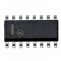
MC74ACT259DG ON Semiconductor, MC74ACT259DG Datasheet

MC74ACT259DG
Specifications of MC74ACT259DG
Related parts for MC74ACT259DG
MC74ACT259DG Summary of contents
Page 1
MC74AC259, MC74ACT259 8−Bit Addressable Latch The MC74AC259/74ACT259 is a high−speed 8−bit addressable latch designed for general purpose storage applications in digital systems multifunctional device capable of storing single line data in eight addressable latches, and also a ...
Page 2
MODE SELECT−FUNCTION TABLE Inputs Operating Mode Master Reset Demultiplex (Active HIGH • • Decoder when • • • • ...
Page 3
MC74AC259, MC74ACT259 NOTE: This diagram is provided only for the understanding of logic operations and should not be used to estimate propagation delays. Figure 3. Logic Diagram http://onsemi.com ...
Page 4
MAXIMUM RATINGS Symbol V DC Supply Voltage (Referenced to GND Input Voltage (Referenced to GND Output Voltage (Referenced to GND) OUT I DC Input Current, per Pin Output Sink/Source Current, per ...
Page 5
DC CHARACTERISTICS Symbol Parameter V Minimum High Level IH Input Voltage V Maximum Low Level IL Input Voltage V Minimum High Level OH Output Voltage V Maximum Low Level OL Output Voltage I Maximum Input IN Leakage Current I †Minimum ...
Page 6
... AC CHARACTERISTICS (For Figures and Waveforms − See Section 3 of the ON Semiconductor FACT Data Book, DL138/D) Symbol Parameter Propagation Delay t PLH Propagation Delay t PHL Propagation Delay t PLH Propagation Delay t PHL Propagation Delay t PLH Address Propagation Delay t PHL Address Propagation Delay t PHL *Voltage Range 3 3.3 V ±0.3 V. ...
Page 7
... CC Supply Current *All outputs loaded; thresholds on input associated with output under test. †Maximum test duration 2.0 ms, one output loaded at a time. AC CHARACTERISTICS (For Figures and Waveforms − See Section 3 of the ON Semiconductor FACT Data Book, DL138/D) Symbol Parameter Propagation Delay t PLH ...
Page 8
AC OPERATING REQUIREMENTS Symbol Parameter Setup Time, HIGH or LOW Hold Time, HIGH or LOW Setup Time t s Address to E Hold Time t h Address to ...
Page 9
... MC74AC259DR2 MC74AC259DR2G MC74AC259M MC74AC259MG MC74AC259MEL MC74AC259MELG MC74ACT259N MC74ACT259NG MC74ACT259D MC74ACT259DG MC74ACT259DR2 MC74ACT259DR2G †For information on tape and reel specifications, including part orientation and tape sizes, please refer to our Tape and Reel Packaging Specifications Brochure, BRD8011/D. MC74AC259, MC74ACT259 MARKING DIAGRAMS SO−16 AC259G AWLYWW ...
Page 10
0.25 (0.010) M −A− −B− −T− SEATING PLANE 0.25 (0.010 MC74AC259, MC74ACT259 PACKAGE ...
Page 11
... E L DETAIL P VIEW American Technical Support: 800−282−9855 Toll Free USA/Canada Japan: ON Semiconductor, Japan Customer Focus Center 2−9−1 Kamimeguro, Meguro−ku, Tokyo, Japan 153−0051 Phone: 81−3−5773−3850 http://onsemi.com 11 NOTES: 1. DIMENSIONING AND TOLERANCING PER ANSI Y14.5M, 1982. ...


