MC74HC589ADTR2G ON Semiconductor, MC74HC589ADTR2G Datasheet - Page 3
MC74HC589ADTR2G
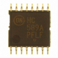
Manufacturer Part Number
MC74HC589ADTR2G
Description
IC SHIFT REGISTER 8BIT 16-TSSOP
Manufacturer
ON Semiconductor
Series
74HCr
Datasheet
1.MC74HC589ADTR2G.pdf
(14 pages)
Specifications of MC74HC589ADTR2G
Logic Type
Shift Register
Output Type
Standard
Number Of Elements
1
Number Of Bits Per Element
8
Function
Universal
Voltage - Supply
2 V ~ 6 V
Operating Temperature
-55°C ~ 125°C
Mounting Type
Surface Mount
Package / Case
16-TSSOP
Lead Free Status / RoHS Status
Lead free / RoHS Compliant
Other names
MC74HC589ADTR2G
MC74HC589ADTR2GOSTR
MC74HC589ADTR2GOSTR
Available stocks
Company
Part Number
Manufacturer
Quantity
Price
Company:

Part Number:
MC74HC589ADTR2G
Manufacturer:
ON
Quantity:
1 000
Company:
Part Number:
MC74HC589ADTR2G
Manufacturer:
ON Semiconductor
Quantity:
74 238
Part Number:
MC74HC589ADTR2G
Manufacturer:
ON/安森美
Quantity:
20 000


Î Î Î Î
Î Î Î Î
Î Î Î Î
Î Î Î Î
Î Î Î Î
Î Î Î Î
Î Î Î Î
Î Î Î Î
Î Î Î Î
Î Î Î Î
Stresses exceeding Maximum Ratings may damage the device. Maximum Ratings are stress ratings only. Functional operation above the
Recommended Operating Conditions is not implied. Extended exposure to stresses above the Recommended Operating Conditions may affect
device reliability.
1. Tested to EIA/JESD22-A114-A.
2. Tested to EIA/JESD22-A115-A.
3. Tested to JESD22-C101-A.
4. Tested to EIA/JESD78.
5. For high frequency or heavy load considerations, see the ON Semiconductor High-Speed CMOS Data Book (DL129/D).
6. Unused inputs may not be left open. All inputs must be tied to a high-logic voltage level or a low-logic input voltage level.
RECOMMENDED OPERATING CONDITIONS
MAXIMUM RATINGS
Symbol
Symbol
V
V
V
I
I
I
I
T
T
T
q
P
MSL
F
V
I
V
V
V
T
t
in
out
CC
GND
Latchup
r
JA
, t
out
STG
L
J
R
out
A
CC
in
D
ESD
CC
in
,
f
Î Î Î Î Î Î Î Î Î Î Î Î Î Î Î Î Î Î Î Î Î
Î Î Î Î Î Î Î Î Î Î Î Î Î Î Î Î Î Î Î Î Î
Î Î Î Î Î Î Î Î Î Î Î Î Î Î Î Î Î Î Î Î Î
Î Î Î Î Î Î Î Î Î Î Î Î Î Î Î Î Î Î Î Î Î
Î Î Î Î Î Î Î Î Î Î Î Î Î Î Î Î Î Î Î Î Î
Î Î Î Î Î Î Î Î Î Î Î Î Î Î Î Î Î Î Î Î Î
Î Î Î Î Î Î Î Î Î Î Î Î Î Î Î Î Î Î Î Î Î
Î Î Î Î Î Î Î Î Î Î Î Î Î Î Î Î Î Î Î Î Î
Î Î Î Î Î Î Î Î Î Î Î Î Î Î Î Î Î Î Î Î Î
Î Î Î Î Î Î Î Î Î Î Î Î Î Î Î Î Î Î Î Î Î
DC Supply Voltage
DC Input Voltage
DC Output Voltage
DC Input Current, per Pin
DC Output Current, per Pin
DC Supply Current, V
DC Ground Current per Ground Pin
Storage Temperature Range
Lead Temperature, 1 mm from Case for 10 Seconds
Junction Temperature Under Bias
Thermal Resistance
Power Dissipation in Still Air at 85_C
Moisture Sensitivity
Flammability Rating
ESD Withstand Voltage
Latchup Performance
DC Supply Voltage
DC Input Voltage, Output Voltage
Operating Temperature, All Package Types
Input Rise and Fall Time
(Figure 3)
CC
and GND Pins
Parameter
Parameter
Above V
http://onsemi.com
MC74HC589A
CC
and Below GND at 85_C (Note 4)
Charged Device Model (Note 3)
Human Body Model (Note 1)
3
Oxygen Index: 30% - 35%
Machine Model (Note 2)
(Referenced to GND)
(Referenced to GND)
(Referenced to GND)
(Referenced to GND)
(Referenced to GND)
V
V
V
V
CC
CC
CC
CC
TSSOP
TSSOP
= 2.0 V
= 3.0 V
= 4.5 V
= 6.0 V
SOIC
SOIC
PDIP
PDIP
Î Î Î Î Î
Î Î Î Î Î
Î Î Î Î Î
Î Î Î Î Î
Î Î Î Î Î
Î Î Î Î Î
Î Î Î Î Î
Î Î Î Î Î
Î Î Î Î Î
Î Î Î Î Î
UL 94 V-0 @ 0.125 in
*55
*0.5 v V
*0.5 v V
Min
2.0
0
0
0
0
*0.5 to )7.0
*65 to )150
Level 1
u4000
u1000
Value
)150
u200
$300
$20
$35
$75
$75
260
112
148
750
500
450
78
Î Î Î Î
Î Î Î Î
Î Î Î Î
Î Î Î Î
Î Î Î Î
Î Î Î Î
Î Î Î Î
Î Î Î Î
Î Î Î Î
Î Î Î Î
CC
CC
)0.5
)0.5
)125
1000
Max
V
800
500
400
6.0
CC
Î Î Î
Î Î Î
Î Î Î
Î Î Î
Î Î Î
Î Î Î
Î Î Î
Î Î Î
Î Î Î
Î Î Î
_C/W
Unit
Unit
mW
mA
mA
mA
mA
mA
_C
_C
_C
_C
ns
V
V
V
V
V
V
Related parts for MC74HC589ADTR2G
Image
Part Number
Description
Manufacturer
Datasheet
Request
R

Part Number:
Description:
ON Semiconductor [VOLTAGE REGULATOR]
Manufacturer:
ON Semiconductor
Datasheet:
Part Number:
Description:
357-036-542-201 CARDEDGE 36POS DL .156 BLK LOPRO
Manufacturer:
ON Semiconductor
Datasheet:
Part Number:
Description:
357-036-542-201 CARDEDGE 36POS DL .156 BLK LOPRO
Manufacturer:
ON Semiconductor
Datasheet:
Part Number:
Description:
357-036-542-201 CARDEDGE 36POS DL .156 BLK LOPRO
Manufacturer:
ON Semiconductor
Datasheet:
Part Number:
Description:
357-036-542-201 CARDEDGE 36POS DL .156 BLK LOPRO
Manufacturer:
ON Semiconductor
Datasheet:
Part Number:
Description:
357-036-542-201 CARDEDGE 36POS DL .156 BLK LOPRO
Manufacturer:
ON Semiconductor
Datasheet:
Part Number:
Description:
357-036-542-201 CARDEDGE 36POS DL .156 BLK LOPRO
Manufacturer:
ON Semiconductor
Datasheet:
Part Number:
Description:
357-036-542-201 CARDEDGE 36POS DL .156 BLK LOPRO
Manufacturer:
ON Semiconductor
Datasheet:
Part Number:
Description:
357-036-542-201 CARDEDGE 36POS DL .156 BLK LOPRO
Manufacturer:
ON Semiconductor
Datasheet:
Part Number:
Description:
357-036-542-201 CARDEDGE 36POS DL .156 BLK LOPRO
Manufacturer:
ON Semiconductor
Datasheet:
Part Number:
Description:
357-036-542-201 CARDEDGE 36POS DL .156 BLK LOPRO
Manufacturer:
ON Semiconductor
Datasheet:
Part Number:
Description:
Manufacturer:
ON Semiconductor
Datasheet:
Part Number:
Description:
Manufacturer:
ON Semiconductor
Datasheet:
Part Number:
Description:
Manufacturer:
ON Semiconductor
Datasheet: