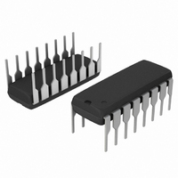
MC74HC595ANG ON Semiconductor, MC74HC595ANG Datasheet - Page 2

MC74HC595ANG
Manufacturer Part Number
MC74HC595ANG
Description
IC SHIFT REGISTER 8BIT 3ST 16DIP
Manufacturer
ON Semiconductor
Series
74HCr
Type
Not Requiredr
Specifications of MC74HC595ANG
Logic Type
Shift Register
Output Type
Standard
Number Of Elements
1
Number Of Bits Per Element
8
Function
Serial to Parallel
Voltage - Supply
2 V ~ 6 V
Operating Temperature
-55°C ~ 125°C
Mounting Type
Through Hole
Package / Case
16-DIP (0.300", 7.62mm)
Counting Sequence
Serial to Serial/Parallel
Number Of Circuits
2
Logic Family
74HC
Propagation Delay Time
140 ns, 100 ns, 28 ns, 24 ns
Supply Voltage (max)
6 V
Maximum Operating Temperature
+ 125 C
Minimum Operating Temperature
- 55 C
Mounting Style
Through Hole
Operating Supply Voltage
2 V to 6 V
Circuit Type
Low-Power Schottky
Current, Supply
160 μA
Function Type
8-Bits
Logic Function
Register
Package Type
PDIP-16
Special Features
Tri-State
Temperature, Operating, Range
-55 to +125 °C
Voltage, Supply
2 to 6 V
Technology
CMOS
Number Of Elements
1
Number Of Bits
8
Logical Function
Shift Register
Operating Supply Voltage (typ)
2.5/3.3/5V
Operating Temp Range
-55C to 125C
Operating Supply Voltage (min)
2V
Operating Supply Voltage (max)
6V
Operating Temperature Classification
Military
Mounting
Through Hole
Pin Count
16
Lead Free Status / RoHS Status
Lead free / RoHS Compliant
Other names
MC74HC595ANGOS
Available stocks
Company
Part Number
Manufacturer
Quantity
Price
Company:
Part Number:
MC74HC595ANG
Manufacturer:
ON
Quantity:
2 000
†For information on tape and reel specifications, including part orientation and tape sizes, please refer to our Tape and Reel Packaging
*This package is inherently Pb−Free.
ORDERING INFORMATION
Specifications Brochure, BRD8011/D.
MC74HC595AN
MC74HC595ANG
MC74HC595AD
MC74HC595ADG
MC74HC595ADR2
MC74HC595ADR2G
MC74HC595ADT
MC74HC595ADTR2
MC74HC595ADTR2G
MC74HC595AFEL
MC74HC595AFELG
GND
Q
Q
Q
Q
Q
Q
Q
B
C
D
E
G
H
F
PIN ASSIGNMENT
1
2
3
4
5
6
7
8
Device
16
15
14
13
12
11
10
9
V
Q
A
OUTPUT ENABLE
LATCH CLOCK
SHIFT CLOCK
RESET
SQ
CC
A
H
SERIAL
INPUT
http://onsemi.com
DATA
OUTPUT
ENABLE
CLOCK
CLOCK
RESET
LATCH
SHIFT
TSSOP−16*
TSSOP−16*
TSSOP−16*
SOEIAJ−16
SOEIAJ−16
(Pb−Free)
(Pb−Free)
(Pb−Free)
(Pb−Free)
(Pb−Free)
Package
PDIP−16
PDIP−16
SOIC−16
SOIC−16
SOIC−16
SOIC−16
A
2
14
10
12
13
11
REGISTER
SHIFT
LOGIC DIAGRAM
LATCH
2500 Tape & Reel
2500 Tape & Reel
2500 Tape & Reel
2500 Tape & Reel
2000 Tape & Reel
2000 Tape & Reel
500 Units / Rail
500 Units / Rail
48 Units / Rail
48 Units / Rail
96 Units / Rail
V
GND = PIN 8
Shipping
CC
15
1
2
3
4
5
6
7
9
= PIN 16
Q
Q
Q
Q
Q
Q
Q
Q
SQ
A
B
C
D
E
F
G
H
H
†
OUTPUT
PARALLEL
OUTPUTS
SERIAL
DATA
DATA


